Monash College scientists have shown a new, strange method for safeguarding molecularly slim gadgets: adding vibrations to lessen vibrations.
Graphene gadgets are coated with a gallium-oxide defensive coating by “pressing” a thin drop of fluid gallium.
This oxide is incredibly thin—less than 100 iotas—yet covers vast scopes, making it potentially relevant for modern massive scope creation.Current, boondocks “2nm” semiconductors from IBM use doors of comparable thickness, near 10nm (140 iotas).
“Precisely moving such a huge region of nanosheets is very novel,” says lead creator Matthew Gebert.
The oxide provides another strategy for device security while also improving device performance:
“The oxide not only improves and safeguards our gadgets when we first exchange it, but also later, during ensuing handling and creation,” says co-creator Semonti Bhattacharyya.
Gallium-oxide’s upgrade is expected to some extent due to the material’s high-K dielectric properties, which play an important role in the long journey toward shrinking gadgets and reducing power waste.
Fluid metal rolling: how to precisely move a defensive, large region of gallium-oxide onto your semiconductors.
Defensive gallium-oxide also produces an excellent result, lowering the electrical opposition in graphene caused by warm vibrations caused by heat in the surrounding materials.
“That is amazing on the grounds that basically we are really adding additional vibrations to lessen all the vibrations,” says Matt.
This is the first time a system to lessen the opposition because of warm vibrations has been shown in a graphene gadget.
Security from a harmful climate
The Monash group from the Bend Focus of Greatness in Future Low-Energy Gadget Advances (Armada) utilized a clever fluid metal printing method to make gallium-oxide (Ga2O3) glass. This strategy was planned by Armada partners at RMIT, who have involved the clever glass in an assortment of gadget applications.
The glass film that structures on the outer layer of drops of fluid gallium metal is in excess of multiple times more slender than a human hair, yet it can be dependably “printed” from the outer layer of the fluid metal to shape uniform nonstop layers over centimeter-sized regions.
The fluid metal strategy offers two benefits for safeguarding gadgets. The layer-printing strategy forestalls development harm, while the moved layer is a decent boundary for additional handling.
Gallium-oxide epitome offers security yet can likewise improve execution due to its high-K dielectric characteristics. High-K dielectrics have not been difficult to coordinate with graphene, as the development of these materials frequently involves the siege of profoundly fiery iotas.
As gallium-oxide epitome is a mechanical exchange strategy (“think forklift stacking,” says Matthew Gebert), it is generally unique to elective testimony techniques (like nuclear layer statements, vanishing, faltering, and fume testimony), which have unwanted traits like high temperature necessities.
Since gallium metal is fluid near room temperature (30 degrees C), this interaction enjoys a ton of benefits for modern reception. In fact, gallium-oxide can be used as a cradle layer before further processing using these various methods.
The Monash group showed that gallium-oxide shielded the graphene from surface harm by testing their graphene gadgets with modern development apparatuses. Saving another oxide layer harmed just the revealed areas of graphene, while the areas that were covered by gallium-oxide held their characteristics.
Dielectric layers and their significance in figuring
Electrically-protecting (dielectric) materials are especially significant in the capability of semiconductors, the tiny “switches” at the core of gadgets and figures. These dielectric materials permit a semiconductor to turn on or off without spilling power, which thus permits you to utilize your telephone or PC.
To “switch” a semiconductor, electrons gather across the dielectric material to make a voltage and impact the gadget. However, thinner dielectrics release flow, reducing switch capacity and wasting flow as intensity.High-K dielectrics are important because they improve the switch’s viability, allowing for less flow spillage and thus less energy waste.
In any case, even high-K dielectrics are not impenetrable to measurement. As electronic materials get more modest and more slender as we steadily walk towards packing in additional semiconductors (to submit to Moore’s Regulation), materials become firmly affected by the surfaces of adjoining materials, frequently bringing about a drop in execution. This makes sense given why graphene is often harmed by high-K dielectrics.
Material vibration is one of these demeaning peculiarities that occur at surfaces.
The advantages of vibrations and gallium-oxide
The vibrations of materials because of their intensity, which cause electrical opposition in materials, are called phonons. These vibrations (phonons) make the iotas sway, and streaming electrons bob off these motions and shift their course, prompting electrical opposition.
The warm vibrations of the carbon iotas in graphene itself cause strikingly little opposition, which is one motivation behind why graphene is such a helpful material for gadgets.
Nonetheless, because graphene is so thin (only one iota thick), warm vibrations in surrounding (remote) materials can generally affect electrons in graphene, and these are the primary reasons for electrical opposition in graphene at room temperature.
As temperatures heat up, more phonons are energized, expanding the opposition by dispersing electrons.
“You can think of this situation as a wall,” says Matt Gebert, a Ph.D. candidate at Monash College/Armada.
“The wall (the 2D graphene) is impacted by the activities of neighbors on the two sides (the protecting materials on one or the other side of graphene). One neighbor may have a perfect climate on their side of the wall (a good cover with few phonons), while the other neighbor may have a crowded nursery that harms the wall (a bad encasing area of strength for with).
“So eventually, your wall (graphene) doesn’t fill the need it was planned to, maybe not in any event, framing a total wall (electronic circuit) any longer.”
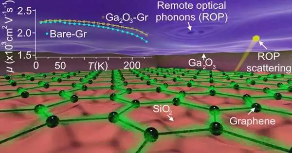
To examine the defensive characteristics of the gallium oxide, the group precisely moved huge regions onto graphene gadgets.
Ensuing estimations affirmed that graphene’s electronic properties at different temperatures and electron populations were kept up with, i.e., high electron portability (a helpful property of a semiconductor) was saved.
“Surprisingly, adding the layer of Ga2O3 glass reduces the electrical opposition in graphene, which is expected to cause phonon dispersal,” Matt explains.(This is valid in an objective scope of temperatures, which is somewhat below room temperature.)
“This is strange, on the grounds that by adding this material, you are presenting extra phonons.” So you could think: “The more phonons, the higher we would anticipate that opposition should be.”
In any case, these outcomes truly do concur with existing hypotheses of phonons in covers. Ga2O3 has solid phonons, yet this equivalent property likewise permits it to change its own nuclear setup to “screen” the electric field from phonons in the silicon-dioxide glass on the opposite side of graphene.
Further aiding what is going on, areas of strength for the phonons are modes that require high energy to populate. Thus, Ga2O3 phonons just become dynamic at higher temperatures (with more nuclear power), and this results in lower generalized opposition in graphene until a temperature of -53 degrees C (220 K). Gallium-oxide is getting just the right vibrations.
New roads to gadget execution
This system for reducing overall phonon content is demonstrated in an interesting way and could be used to identify better-performing mixture materials at room temperature for 2D devices.
A comparable dielectric material with higher-energy phonon modes than Ga2O3 could work well with existing silicon innovations, which are right now being pushed to their quantum-scale limits.
The fluid metal printing strategy is a flexible technique for modern accomplices. The cycle for contact printing Ga2O3 scales to huge wafer-scale regions is truly automatable and has shown great reproducibility, demonstrating its legitimacy for industry adoption.
Gallium metal, which softens at around 30 degrees C, and the exchange gear are likewise modest compared with other oxide affidavit techniques, which require a lot of material or profoundly raised temperatures.
“Passivating graphene and suppressing interfacial phonon dispersing with precisely moved Ga2O3” was distributed in Nano Letters.
More information: Matthew Gebert et al, Passivating Graphene and Suppressing Interfacial Phonon Scattering with Mechanically Transferred Large-Area Ga2O3, Nano Letters (2022). DOI: 10.1021/acs.nanolett.2c03492
Journal information: Nano Letters


