Modern electronic, photonic, photovoltaic, thermoelectric, and a plethora of other semiconductor devices are built on semiconductor materials, which are essential to the production of gadgets, automobiles, computers, mobile phones, and other equipment.
The vast majority of all semiconductor gadgets are made of or on silicon wafers. Novel gathering IV semiconductor epitaxial structures made out of silicon, germanium, carbon, or tin on silicon or silicon-on-separator wafers give a characteristic course to proceed with the progress of the properties of cutting-edge silicon gadgets with upgraded or arising one-of-a-kind properties.
Carriers’ mobility
One of the most important quality measures of any semiconductor material is the mobility of free carriers in conduction (electrons) or valance (holes) bands, along with a relatively large energy bandgap. This determines whether or not the material is suitable for use in a wide range of classical electronic, optoelectronic, and sensor devices, as well as for novel applications in emerging quantum devices.
Higher portability empowers quicker activity of a gadget at lower power utilization and, in this way, prompts diminished Joule heat dispersal, which is fundamental for scaling and speeding up current electronic gadgets. It is even more crucial for electronics and devices that operate at cryogenic temperatures and are designed to control quantum processors’ distributed registers. Likewise, transporter versatility is a basic quality for quantum gadgets, frequently playing a critical role in new revelations.
Strained germanium semiconductor
Since the invention of the first transistor, the semiconductor material germanium has been utilized in industry. It has some advantages over silicon, other semiconductors, and III-V compounds. Particularly, the creation of novel quantum materials with distinctive properties may be possible if strain engineering can improve the mobility of germanium’s holes. Quantum materials will be materials that display novel electronic and attractive properties because of their quantum nature, and they are being read up for many applications, including quantum registering, detecting, and energy stockpiling.
Due to the misalignment of the components’ crystal lattices, semiconductor heterostructures on silicon have a built-in strain. It is a crucial parameter used in material energy band structure engineering. However, in order to overcome a number of significant obstacles in the heteroepitaxy of these materials, research and development of high-mobility strained silicon, silicon-germanium, and germanium heterostructures require special epitaxial growth techniques like molecular beam epitaxy and chemical vapor deposition, in addition to epitaxy knowledge and technologies.
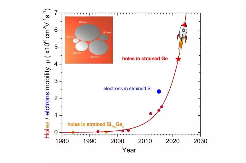
The notable development of the openings and electromagnetic mobilities in the gathering of IV semiconductors at low temperatures The work’s result is indicated by the star. Credit: Maksym Myronov
Long-looked-for mix of boundaries in a single material framework
In our new article, distributed in the journal Little Science, a worldwide group of specialists from the U.K. and, furthermore, Canada provided details regarding a record-high portability of openings, arriving at 4.3 million cm2V-1s-1 in an epitaxially stressed germanium semiconductor, developed on a standard silicon wafer. This critical increment of versatility by more than four times, contrasted with the cutting edge, permits openings to beat electrons in the gathering of IV semiconductor materials. The best electron mobility that has been reported for the most recent strained silicon is twice as high as the demonstrated hole mobility in strained germanium. Any other semiconductor material system has not experienced a situation that is comparable to this one.
Notwithstanding the record portability, this material stage uncovers a one-of-a kind blend of properties, which are an extremely enormous and compelling g*-factor, a low permeation thickness, and a little successful mass. Quantum electronic circuits based on spin qubits, including devices for Majorana Fermions, as well as the research and development of low-temperature electronics with reduced Joule heating, depend on this long-awaited combination of parameters in a single material system.
The modern epitaxial growth technique that led to the superior monocrystalline quality of the strained germanium material system with a very low density of background impurities and other imperfections was the driving force behind this significant advance. New opportunities for innovative quantum device technologies and applications in quantum as well as classical electronics, optoelectronics, and sensors will result from this superior material system’s unique combination of properties. Specifically, the blend of gotten boundaries will work with the acknowledgment of the predominant quality along the side gated quantum gadgets. In addition, these hole properties can be accurately simulated and predicted, reducing the need for costly and lengthy experimental trial-and-error experiments.
When compared to other materials
This achievement narrows the gap between the best hole mobility of gallium arsenide heterostructures grown on the same material substrate, which had previously increased to 5.8 million cm2V-1s-1. Tragically, III-V materials are muddled to process, costly, not broadly plentiful in the world’s hull compared with silicon and germanium, don’t exist in isotopically unadulterated structures, and are not viable with the cutting-edge silicon advancements for large-scale manufacturing. Perovskites, 2D materials, and all other known semiconductors, including III-V and II-VI, show significantly reduced hole mobility in comparison to the strained germanium and gallium arsenide heterostructures.
We accept that the greatest portability has still not been achieved in the stressed germanium heterostructures, and there is space for additional enhancements. To truly comprehend the microscopic mechanisms that restrict hole mobility, more in-depth experimental and theoretical research is clearly required.
In general, this breakthrough in increasing the mobility of holes in strained germanium may have significant repercussions for the creation of novel quantum technologies and materials. In the years to come, it will be exciting to see how this research develops and what new applications emerge.
More information: Maksym Myronov et al, Holes Outperform Electrons in Group IV Semiconductor Materials, Small Science (2023). DOI: 10.1002/smsc.202200094


