The ability to send and control the smallest unit of light, the photon, with negligible error, plays an important role in optical correspondences as well as plans for quantum PCs that would use light rather than electric charges to store and convey data.
Currently, scientists at the National Institute of Standards and Technology (NIST) and their collaborators have linked, on a single CPU, quantum dab—fake iotas that create individual photons quickly and on-request when illuminated by a laser—with small circuits that can direct the light without a significant deficiency of force.
To make the super-low-misfortune circuits, the analysts created silicon-nitride waveguides—tthe channels through which the photons voyaged—aand covered them in silicon dioxide. The channels were wide yet shallow, which decreased the probability that photons would disperse out of the waveguides. Making the waveguides out of silicon dioxide also helped to reduce dispersion.
The researchers revealed that their model circuits have a deficiency of force equivalent to only one percent of comparable circuits that also utilize quantum dots and were created by different groups.
At last, gadgets that integrate this new chip innovation could exploit the odd properties of quantum mechanics to perform complex calculations that old-style (non-quantum) circuits may not have the capacity to do.
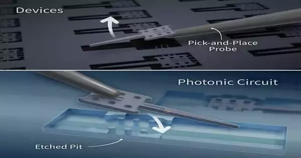
Outline depicts a portion of the steps taken to create the new super-low-misfortune photonic circuit on a chip.A microprobe lifts a gallium arsenide gadget containing a quantum dab—fake iotas that create single photons—from one chip. Then the test puts the quantum-dab gadget on a low-misfortune silver-nitride waveguide based on another chip. Credit: S. Kelley/NIST
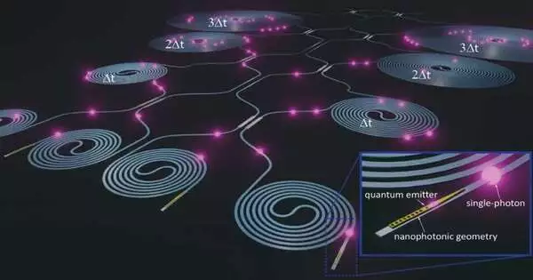
For example, as per the laws of quantum mechanics, a solitary photon has a likelihood of living in two better places, like two unique waveguides, simultaneously. Those probabilities can be utilized to store data; a singular photon can go about as a quantum bit, or qubit, which conveys considerably more data than the double piece of an old-style PC, which is restricted to a value of 0 or 1.
To perform tasks critical for addressing computational issues, these photon qubits—all of which travel at the same speed and are indistinguishable from one another—must appear at explicit handling hubs in the circuit.That is a test because photons coming from various locations and traveling through various waveguides across the circuit may end up in essentially various good places from handling focuses.To guarantee concurrent appearance, photons produced nearer to the assigned objective should defer their excursion, giving those that lie in additional far-off waveguides an early advantage.
The circuit concocted by NIST scientists including Ashish Chanana and Marcelo Davanco, along with a global group of partners, considers huge time delays since it utilizes waveguides of different lengths that can store photons for somewhat extensive stretches of time. For example, the scientists compute that a 3-meter-long waveguide (firmly wound so its width on a chip is a couple of millimeters) would have a 50 percent likelihood of sending a photon with a delay of 20 nanoseconds (billionths of a second). By correlation, past gadgets, created by different groups and working under comparable circumstances, were restricted to inciting time delays of just a single 100th as lengthy.
The longer delay times accomplished with the new circuit are likewise significant for tasks in which photons from at least one quantum dot need to show up at a particular area at similarly divided time spans. Likewise, the low-misfortune quantum-dab circuit could decisively increase the quantity of single photons accessible for conveying quantum data on a chip, empowering bigger, speedier, and more solid computational and data handling frameworks.
The researchers, who incorporate analysts from the College of California, Santa Barbara (UCSB), the Massachusetts Foundation for Innovation (MIT), the Korea Organization of Science and Innovation, and the College of So Paulo in Brazil, revealed their discoveries on December 11 in Nature Correspondences.
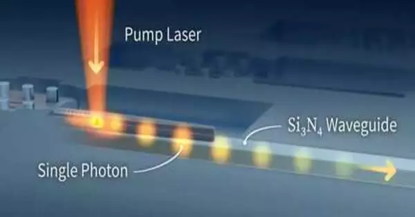
Laser light beaming on the quantum dots triggers them to create a progression of single photons that move through the silicon nitride waveguide.
The mixture circuit comprises two parts, each initially based on a different chip. One, a gallium arsenide semiconductor gadget planned and created at NIST, has the quantum dots and straightforwardly pipes the single photons they produce into a subsequent gadget—a low-misfortune silicon nitride waveguide created at UCSB.
Scientists at MIT first used the fine metal tip of a pick-and-spot microprobe, which behaved like a small crowbar, to pry the gallium arsenide device from the chip created at NIST.They then positioned it on the silicon nitride circuit on the other chip.
The scientists face a few difficulties before the mixture circuit can be regularly utilized in a photonic gadget. As of now, around 6% of the singular photons created by the quantum dab can be piped into the circuit. However, assuming the group changes the location where the photons are piped, the rate could increase by more than 80% when combined with upgrades in the positioning and direction of the quantum dabs.
Another issue is that the quantum dabs don’t necessarily radiate single photons at the same frequency, a prerequisite for making the vague photons vital for the quantum computational tasks. The group is investigating a few systems, including applying a steady electric field to the dabs, that might ease that issue.
More information: Ashish Chanana et al, Ultra-low loss quantum photonic circuits integrated with single quantum emitters, Nature Communications (2022). DOI: 10.1038/s41467-022-35332-z
Journal information: Nature Communications


