The far and wide utilization of electronic gadgets to cooperate with others and access the web has expanded the requirement for profoundly performing correspondence advancements that can send information quicker and all the more effectively. Expanding the information transmission pace of gadgets without unfavorably influencing their energy effectiveness, notwithstanding, is a difficult undertaking.
Scientists at the College of Southampton in the UK have as of late fostered a promising new transmitter in view of reciprocal metal-oxide semiconductor (CMOS) innovation and silicon photonics. This transmitter, presented in Nature Hardware, was found to accomplish surprising information transmission rates while consuming negligible energy.
“The coordination of silicon photonics with hardware is fundamental for creating viable frameworks for various applications,” David J. Thomson, one of the creators of the paper, told Tech Xplore.
“Our belief is that sophisticated CMOS design methods can be employed to create photonics devices and electronics and photonics devices as integrated functional modules. These modules could then be utilized to realize different signal processing functions (like complex signal formatting, spectral synthesis, and signal equalization) within optical to electrical or electrical to optical conversion processes.”
David J. Thomson, one of the authors of the paper,
“The blend of the optical modulator and its electronic drive enhancer is a key electronic-photonic interface frequently directing framework execution regarding pace and power utilization and subsequently making an ideal point of interaction of these two parts was distinguished as a significant examination heading for us, tracing all the way back to the year 2010.”
At first, Thomson and his partners attempted to foster their transmitter utilizing a more ordinary methodology, which involves planning electrical driver intensifiers and optical modulators independently and then, in this manner, joining them. In this manner, they explored different avenues regarding various answers for electrically associating these two parts, for example, wire holding and flip-chip holding.
Both of these strategies didn’t prompt the outcomes they were expecting; hence, they chose to go beyond the ‘customary’ approach for planning transmitters. In particular, they took on an elective strategy that includes co-planning the electrical driver speaker and optical modulator inside the gadget.
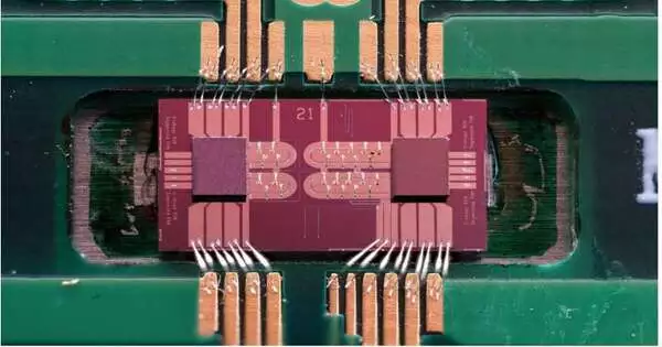
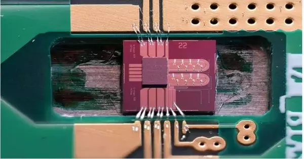
Photo of PAM-4 transmitter including two CMOS electronic drivers flip-chip reinforced onto a silicon photonic modulator. Credit: Li et al.
“Taking on our co-plan approach, we fostered a demonstrating technique that had the option to integrate all components of the incorporated transmitter,” Thomson made sense of.
“Definite reenactments showed that to deliver a huge balance profundity from the optical gadget, its radio recurrence reaction ought to be changed utilizing electronic inductive designs to such an extent that the electrical drive flow is proficiently utilized. The CMOS electronic driver chip was consequently planned with the expected usefulness to repay transmission capacity limits of the modulator.”
Utilizing their proposed plan system, the specialists made a transmitter with a moderately sluggish balance that is equipped for a solid tweak contrast, which can send information at high rates. In starting tests, their gadget accomplished a 112 gigabaud each second on-off keying rate and a 224 gigabit each second heartbeat sufficiency regulation.
Astoundingly, the gadget’s energy proficiency was below picojoules per bit. The co-plan approach utilized by Thomson and his partners in this way empowered a high information throughput while diminishing the gadget’s power utilization.
“An elective examination heading in this space is the coordination of outlandish materials with silicon waveguides for improved modulator execution,” Thomson said.
“Nonetheless, CMOS similarity is then lost, confounding courses for high-volume, high return, and minimal expense production. Our work exhibits that there is still an extension for execution enhancements from all-silicon-based gadgets that can be created in a minimal-cost CMOS-like way.”
The new transmitter configuration presented by this group of specialists could, before long, move the advancement of comparative parts toward upgrading interchanges. Generally speaking, their review exhibits the degree to which exceptional plan procedures can assist with supporting the presentation of electronic and photonic gadgets.
“We accept that exceptional CMOS plan strategies could be utilized to create photonics gadgets and fabricate hardware and photonics gadgets as coordinated utilitarian modules, in which different sign handling capabilities (like sign adjustment, complex sign arranging, and ghastly union) could be acknowledged inside electrical to optical or optical to electrical transformation processes,” Thomson added.
“This isn’t to propose that photonics could override hardware, yet that the combination of photonics and gadgets could empower gadget execution past that of standard hardware modules, with regards to speed or data transfer capacity as well as framework intricacy and energy proficiency. We accept that this reconciliation approach could be utilized to accomplish 200 GBaud transmission with a silicon photonic modulator.”
More information: Ke Li et al. An integrated CMOS-silicon photonics transmitter with a 112 gigabaud transmission and picojoule per bit energy efficiency, Nature Electronics (2023). DOI: 10.1038/s41928-023-01048-1


