Two-layered materials, which comprise only a single layer of iotas, can be pressed together more thickly than traditional materials, so they could be utilized to make semiconductors, sunlight-based cells, LEDs, and different gadgets that run quicker and perform better.
One issue keeping these cutting-edge gadgets down is the intensity they produce when being used. Regular gadgets normally arrive at around 80 degrees Celsius, but the materials in 2D gadgets are stuffed so thickly into such a small region that the gadgets can turn out to be two times as hot. This temperature increment can harm the gadget.
This issue is intensified by the fact that researchers don’t have a decent comprehension of how 2D materials grow when temperatures climb. Because the materials are so light and transparent, measuring their warm development coefficient (Sleuth)—the tendency for the material to grow as temperatures rise—is nearly impossible using standard methods.
“People use a scientific ruler or a microscope to assess the thermal expansion coefficient of a bulk material because they have the sensitivity to measure them. Because we cannot see a 2D substance, we must use a different type of ruler to calculate the TEC.”
Yang Zhong, a graduate student in mechanical engineering.
“When people measure the warm development coefficient of a mass material, they use a logical ruler or a magnifying lens on the grounds that mass materials are difficult to quantify. The test with a 2D material is that we can’t actually see them, so we want to go to one more kind of ruler to gauge the Sleuth,” says Yang Zhong, an alumni undergrad in mechanical design.
Zhong is the co-lead creator of an examination paper that shows simply such a “ruler.” As opposed to straightforwardly estimating how the material extends, they use laser light to follow the vibrations of the particles that involve the material. Taking estimations of one 2D material on three unique surfaces, or substrates, permits them to remove its warm development coefficient precisely.
The new review shows that this strategy is exceptionally precise, achieving results that match hypothetical estimations. The methodology affirms that the detectives of 2D materials have a much smaller reach than previously suspected. This data could assist engineers with planning cutting-edge gadgets.
“By affirming this smaller actual reach, we provide engineers with a ton of material adaptability for picking the base substrate when they are planning a gadget.” They do not need to create a new base substrate just to relieve warm pressure.”We accept this has vital ramifications for the electronic gadget and bundling local areas,” says co-lead creator and previous mechanical designing alumni understudy Lenan Zhang SM ’18, Ph.D. ’22, who is currently an exploration researcher.
Co-creators incorporate senior creator Evelyn N. Wang, the Portage Teacher of Designing and head of the MIT Division of Mechanical Designing, as well as others from the Branch of Electrical Designing and Software Engineering at MIT and the Division of Mechanical and Energy Designing at the Southern College of Science and Innovation in Shenzhen, China. The exploration is distributed in Science Advances.
Estimating vibrations
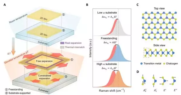
Since 2D materials are so small—mmaybe only a couple of microns in size—sstandard devices aren’t sufficiently delicate to gauge their extension straightforwardly. Furthermore, because the materials are so thin, they should stick to a substrate such as silicon or copper.On the off chance that the 2D material and its substrate have various descriptors, they will extend distinctively when temperatures increment, which causes warm pressure.
When a 2D material is clung to a substrate with a higher Sleuth, for example, when the gadget is warmed, the substrate will extend more than the 2D material, which extends it.This makes it hard to gauge the genuine thickness of a 2D material since the substrate influences its extension.
The scientists defeated these issues by zeroing in on the particles that make up the 2D material. At the point when a material is warmed, its particles vibrate with a lower recurrence and move farther apart, which makes the material extend. They measure these vibrations utilizing a procedure called miniature Raman spectroscopy, which includes stirring things up around town with a laser. The vibrating particles dissipate the laser’s light, and this association can be utilized to distinguish their vibrational recurrence.
In any case, as the substrate extends or packs, it influences how the 2D material’s molecules vibrate. Analysts anticipated decoupling this substrate impact in order to focus on the material’s natural properties.They did this by estimating the vibrational recurrence of similar 2D material on three distinct substrates: copper, which has a high Sleuth; combined silica, which has a low Detective; and a silicon substrate speckled with minuscule openings. Since the 2D material drifts over the openings on the last substrate, they can perform estimations on these little areas of unsupported material.
The scientists then put every substrate on a warm stage to unequivocally control the temperature, warmed each example, and performed miniature Raman spectroscopy.
“By performing Raman estimations on the three examples, we can remove what many refer to as the substrate-subordinate temperature coefficient.””We can separate the natural sleuth of the 2D material by using these three distinct substrates and knowing the detectives of the combined silica and copper,” Zhong explains.
An inquisitive outcome
They played out this examination on a few 2D materials and found that they generally paired hypothetical estimations. In any case, the scientists saw something they didn’t anticipate: 2D materials fell into a progressive system in light of the components that contain them. For example, a 2D material that contains molybdenum generally has a higher strength than one that contains tungsten.
The specialists dug further and discovered that this ordered progression is brought about by a principal nuclear property known as electronegativity. Electronegativity describes the propensity for molecules to pull or concentrate electrons when they are excited. It is recorded on the intermittent table for every component.
They tracked down the fact that the bigger the contrast between the electronegativities of components that structure a 2D material, the lower the material’s warm extension coefficient will be. According to Zhong, a specialist could use this strategy to quickly determine the sleuth for any 2D material, rather than relying on complex computations that would normally require a supercomputer to crunch.
“A designer can simply look through the occasional table, get the electronegativities of the relating materials, plug them into our connection condition, and in no less than a few minutes they can have a sensibly decent assessment of the sleuth.” “This is extremely encouraging for quick material choices for designing applications,” Zhang says.
Pushing ahead, the scientists need to apply their philosophy to a lot more 2D materials, maybe constructing an information base of Sleuths. They likewise need to utilize miniature Raman spectroscopy to gauge the thickness of heterogeneous materials, which join various 2D materials. Also, they desire to gain proficiency with the fundamental reasons why the development of 2D materials is not quite the same as that of mass materials.
More information: Yang Zhong et al, A unified approach and descriptor for the thermal expansion of two-dimensional transition metal dichalcogenide monolayers, Science Advances (2022). DOI: 10.1126/sciadv.abo3783. www.science.org/doi/10.1126/sciadv.abo3783
Journal information: Science Advances


