A group of researchers from Brown University is opening up a new realm of possibilities in the study of these crucial components, which can help power devices like laptops and smartphones, with a new microscopy technique that uses blue light to measure electrons in semiconductors and other nanoscale materials.
The findings are the first of their kind in nanoscale imaging and offer a solution to a problem that has been around for a long time. This problem has made it hard to study important phenomena in a wide range of materials, which could one day lead to semiconductors and electronics that use less energy. The published work in Light: Applications and Science.
“There is a lot of interest these days in studying materials with nanoscale resolution using optics,” said Daniel Mittleman, the author of the paper that describes the work and a professor in Brown’s School of Engineering. As the frequency gets more limited, this turns into much harder to carry out. Since then, no one has ever done it with blue light.”
“There is a lot of interest these days in studying materials with nanoscale resolution using optics. As the wavelength shortens, this becomes much more difficult to implement. As a result, no one has ever done it with blue light until now.”
Daniel Mittleman, a professor in Brown’s School of Engineering and the author of the publication presenting the discovery.
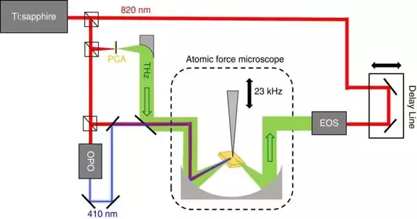
Regularly, when analysts use optics like lasers to study nanoscale materials, they utilize light that transmits long frequencies like red light or infrared. In the study, scattering-type scanning near-field microscopy (s-SNOM) was the method studied. It involves scattering light from a tip that has been sharpened and has a small diameter of a few tens of nanometers. The tip is just slightly above the sample material that needs to be imaged.
When optical light is applied to that sample, it scatters, leaving behind information about the nanometer-sized area of the sample that is directly beneath the tip. The specialists dissect that dispersed radiation to remove data about this little volume of material.
Although the method has been the basis for numerous technological advancements, it is unable to work with light with a much shorter wavelength, such as blue light. This means that since the 1990s, when the method was invented, it has been impossible to use blue light, which is better suited for studying certain materials for which red light is ineffective, to gain new insights from semiconductors that have already been studied.
The Brown researchers explain in the new study how they overcame this obstacle to carry out what is believed to be the very first experimental demonstration of s-SNOM using blue light rather than red.
The researchers used blue light to measure a silicon sample that could not be measured with red light for the experiment. The measurements proved the feasibility of using shorter wavelengths to investigate nanoscale materials.
Mittleman stated, “The match was very good when we were able to compare these new measurements to what one might expect to see from silicon.” It demonstrates that we comprehend how to interpret the results and that our measurement is effective. We can now begin to study all of these materials in a way that we were unable to do before.”
The researchers had to think outside the box to carry out the experiment. In essence, they decided to make things more difficult in order to make things simpler. With the commonplace method, for example, blue light is difficult to utilize in light of the fact that its frequency is so short, implying that centering over the ideal place close to the metal tip is really difficult. On the off chance that not adjusted perfectly, the estimation won’t work. With the red light, this centering condition is more loose, making it simpler to adjust the optics to effectively remove the dispersed light.
The researchers used blue light to not only illuminate the sample so that the light scatters, but also to produce a burst of terahertz radiation from the sample in response to these difficulties. The sample’s electrical properties are important information carried by the radiation.
While the solution eliminates the need to be as precise when aligning the tip over the sample, it adds an additional step and increases the amount of data the scientists must analyze. The key is that terahertz radiation aligns much more easily because it has a longer wavelength.
Mittleman stated, “It still has to be really close, but it doesn’t have to be as close.” You will still be able to obtain information in the terahertz when the light hits it.”
The researchers are eager to see what new information and discoveries the method produces in the future, such as improved understanding of semiconductors used in blue LED technology. Mittleman is currently devising strategies for analyzing materials using blue light in ways that scientists have never been able to do before.
More information: Angela Pizzuto et al, Near-field terahertz nonlinear optics with blue light, Light: Science & Applications (2023). DOI: 10.1038/s41377-023-01137-y


