A new twist on one of the twentieth century’s smallest but grandest inventions, the transistor, could help feed the world’s ever-growing appetite for digital memory while slicing up to 5% of its energy-hungry diet.
Following years of research by Christian Binek of the University of Nebraska–Lincoln and Jonathan Bird and Keke He of the University of Buffalo, the physicists recently collaborated to create the first magneto-electric transistor.
Along with lowering the energy consumption of any microelectronics that incorporate it, the team’s design could reduce the number of transistors required to store specific data by up to 75 percent, according to Nebraska physicist Peter Dowben, resulting in smaller devices. It could also provide those microelectronics with steel-trap memory, which remembers exactly where its users left off, even after being shut down or losing power abruptly.
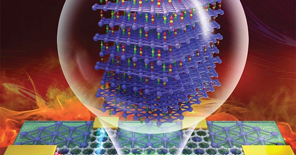
The implications of this most recent demonstration are profound, “said Dowben, who co-authored a recent paper on the work that appeared on the cover of Advanced Materials.
“The traditional integrated circuit is facing some serious problems, There is a limit to how much smaller it can get. We’re basically down to the range where we’re talking about 25 or fewer silicon atoms wide. And you generate heat with every device on an (integrated circuit), so you can’t any longer carry away enough heat to make everything work, either.”
said Dowben, Charles Bessey Professor of physics and astronomy at Nebraska.
Millions of transistors line the surface of every modern integrated circuit, or microchip, which is made in massive quantities—roughly 1 trillion in 2020 alone—from the industry’s favorite semiconducting material, silicon. The tiny transistor, by regulating the flow of electric current within a microchip, effectively acts as a nanoscopic on-off switch that is required for writing, reading, and storing data as the 1s and 0s of digital technology.
However, silicon-based microchips are reaching their practical limits, according to Dowben. Because of these constraints, the semiconductor industry is investigating and funding every promising alternative it can find.
“The traditional integrated circuit is in serious trouble,” said Dowben, the Charles Bessey Professor of Physics and Astronomy at the University of Nebraska. “There is a limit to how small it can become. We’re basically down to the point where we’re talking about silicon atoms that are 25 or fewer wide. And because every device on an integrated circuit generates heat, you can no longer carry away enough heat to keep everything running. “
That problem looms even as demand for digital memory and the energy required to support it has skyrocketed due to the widespread adoption of computers, servers, and the internet. The smartening of TVs, vehicles, and other technology through the use of microchips has only increased that demand.
“We’re getting close to approaching the previous energy consumption of the United States just for memory (alone),” Dowben said. “And it doesn’t stop there.
“So, if at all possible, you need something that you can shrink smaller.” Above all, you need something that works differently than a silicon transistor so that you can significantly reduce power consumption. ” Now that it’s working, the fun can begin. ‘
Typical silicon-based transistors have several terminals. The source and drain are the starting and ending points for electrons flowing through a circuit. Another terminal, the gate, is located above that channel. Voltage applied between the gate and source can determine whether the electric current flows with low or high resistance, resulting in either a buildup or absence of electron charges, which is encoded as a 1 or 0, respectively. However, random-access memory (RAM), on which most computer applications rely, requires a constant supply of power just to keep those binary states alive.
Rather than relying on electric charge as the foundation of its strategy, the researchers turned to spin, a magnetism-related feature of electrons that points up or down and can be interpreted as a 1 or 0, just like an electric charge. The researchers recognized that electrons travelling through graphene, a one-atom-thick ultra-strong material, can preserve their original spin orientations for relatively long distances—an enticing trait for proving the promise of a spintronic-based transistor. Controlling the orientation of those spins while utilizing far less power than a traditional transistor was a considerably more difficult idea.
To accomplish this, the researchers needed to overlay the graphene with the appropriate substance. Binek, fortunately, had already spent years researching and modifying just such a substance, chromium oxide. Crucially, chromium oxide is magneto-electric, which means that by introducing a small amount of transient, energy-sipping voltage, the spins of the atoms at its surface can be changed from up to down or vice versa.
When a positive voltage is applied, the spins of the underlying chromium oxide point up, causing the spin orientation of the graphene’s electric current to veer left and produce a detectable signal. Negative voltage, on the other hand, flips the spins of the chromium oxide down, causing the spin orientation of the graphene’s current to flip to the right and generate a clearly identifiable signal from one end.
“Now you’re starting to get pretty good fidelity (in the signal), because if you’re sitting on one side of the device and apply a voltage, the current will flow this way.” “You may say ‘on,'” Dowben added. However, if it’s commanding the current to travel in the opposite direction, that’s definitely “wrong.”
“This has the potential to provide high quality at a low energy cost. You simply apply electricity, and it flips. “
As exciting and useful as the team’s presentation was, Dowben pointed out that there are lots of alternatives to graphene that share its one-atom thickness but also have features more suitable for a magneto-electric transistor. He claims that the competition to overlay chromium oxide with those other 2D candidates is already underway, and that it signifies “not the end of something, but the beginning of something.”
“Now that it works, the fun begins,” Dowben said. “Everyone will have their own favorite 2D substance, and they’ll try it out.” Some of them will function much, much better than others. However, now that you know it works, it’s worthwhile to invest in those other, more complex materials that could
“Now everyone can get in on the action, figuring out how to make the transistor extremely good and competitive, even exceeding silicon.”
Arriving at that point was a long trip paved with “a gigantic number of breakthroughs,” according to Dowben, particularly from the Binek-Bird duo.
“This type of study highlights how significant and productive collaborative research can be,” Bird said, noting that it “combines Nebraska’s renowned expertise in magnetic materials with Buffalo’s skills in nanoscale semiconductor devices.”
Dowben only mentioned a few of the team’s significant achievements. There was an understanding that magneto-electric materials could be a viable solution. The chemical formula for chromium oxide It was modified to control its spin with voltage rather than power-draining magnetism, as well as to run much above room temperature—because, as Dowben put it, “It can’t just work in Nebraska in the winter if you want to compete with the semiconductor industry.” It must function during the heat in Saudi Arabia. ” Then there were the computer simulations based on theory and the numerous early-stage prototypes.
“There was no Edisonian moment in this room.” As Dowben explained, “You kind of know where you’re headed, but it takes a while.” “There are a lot of technological issues to work out.” It’s a struggle, and it’s not pretty.
But sometimes the results are fantastic,” he explained, “and it’s fun.”
