
Forward leaps in current microelectronics rely upon understanding and controlling the development of electrons in metal. Enlarging the thickness of metal sheets to the requested nanometers can empower choice control over how the metal’s electrons move. Thusly, one can give properties that aren’t found in mass metals, for example, ultrafast conduction of power. Presently, scientists from Osaka University and their teaming up accomplices have blended a clever class of nanostructured superlattices. This study empowers a strangely serious level of command over the development of electrons inside metal semiconductors, which vows to upgrade the usefulness of regular advances.
Working with cutting-edge microelectronic functionalities is still a thriving profession all over the world.A few Nobel prizes have been granted on this point, truth be told. Analysts routinely blend nanostructured superlattices—consistently rotating layers of metals sandwiched together—from materials of a similar aspect, for instance, sandwiched 2D sheets. A vital part of the current scientists’ work is the easy creation of hetero-layered superlattices; for instance, 1D nanoparticle chains sandwiched inside 2D nanosheets.
“Nanoscale hetero-dimensional superlattices are often difficult to construct, but they can display useful physical features such as anisotropic electrical conductivity,” the researchers write.
Yung-Chang Lin
Yung-Chang Lin, senior creator, says “Nanoscale hetero-layered superlattices are commonly difficult to plan, yet can show important actual properties like anisotropic electrical conductivity.” “We fostered a flexible method for planning such designs, and in this manner we will achieve a moving blend of many custom superstructures.”

(a) A traditional superlattice structure model made up of various 2D materials.(b) A recently discovered superlattice structure model is made up of two-layered (film-like) and one-layered (chain-like) materials.Photographer: Y.C. Lin
The scientists involved used compound fume testimony — a typical nanofabrication method in industry — to plan vanadium-based superlattices. These attractive semiconductors show what is known as an “anisotropic odd Hall impact” (AHE), meaning directionally centered charge amassing under in-plane attractive field conditions (in which the regular Hall impact isn’t noticed). Normally, the AHE is noticed exclusively at super low temperatures. In the current examination, the AHE was seen at room temperature and higher, up to around essentially the limit of water. The AHE’s age at viable temperatures will work with its use in regular advance.
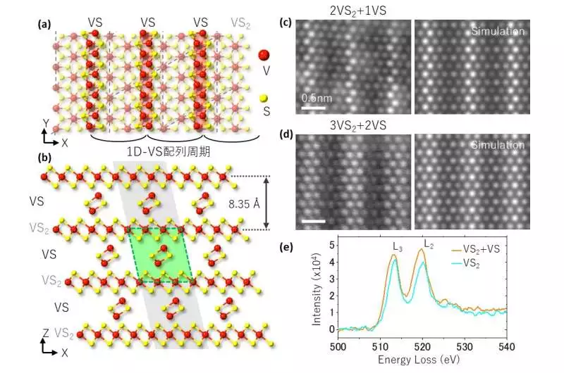
(a) From the top, an atomic model of the stacking design of the VS2-VS superlattice saw.The red and yellow balls address V and S iotas. (b) A side view of the atomic model of the VS2-VS superlattice.The green square shape is the unit cell of the superlattice. (c, d) STEM images of a 2D-film/1D-chain/2D-film (VS2/VS/VS2) superlattice structure and the corresponding mimicked STEM images of a 2D-film/1D-chain/2D-film (VS2/VS/VS2) superlattice structure.(e) electron energy-misfortune close to the edge fine design of the L-edge of the V iota. Photographer: Y.C. Lin
“A vital commitment of nanotechnology is its arrangement of functionalities that you can’t get from mass materials,” states Lin. “Our show of a flighty-odd Hall impact at room temperature or more opens up an abundance of opportunities for future semiconductor innovation, all made available by regular nanofabrication processes.”
The current work will assist with working on the thickness of information stockpiling, the proficiency of lighting, and the speed of electronic gadgets. By exactly controlling the nanoscale design of metals that are usually utilized in industry, analysts will create remarkably flexible innovation that outperforms the usefulness of normal materials.
The article, “Heterodimensional superlattice with room-temperature odd Hall impact,” was published in Nature.
More information: Zheng Liu, Heterodimensional superlattice with room temperature anomalous Hall effect, Nature (2022). DOI: 10.1038/s41586-022-05031-2. www.nature.com/articles/s41586-022-05031-2
Journal information: Nature


