An UNSW paper published recently in Nature Surveys Materials provides an exciting overview of the emerging field of 2D ferroelectric materials with layered van der Waals gem structures, a clever class of low-layered materials that is profoundly intriguing for future nanoelectronics.
Future applications incorporate super low energy gadgets, elite execution, non-unstable information stockpiling, high-reaction optoelectronics, and adaptable (energy-reaping or wearable) hardware.
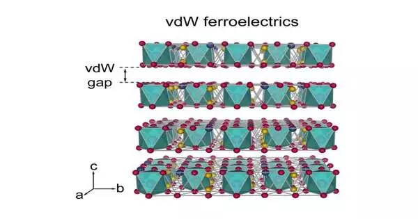
Basically not the same as regular oxide ferroelectrics with unbending grids, van der Waals (vdW) ferroelectrics have stable layered structures with a mix of areas of strength for the interlayer power.
These unique nuclear plans, in combination with the ferroelectric request, lead to new peculiarities and functionalities not tracked down in regular materials.
“Generally, new properties are found when these materials are shed down to molecularly thin layers,” says creator Dr. Dawei Zhang. For instance, the beginning of the polarization and the exchanging systems for the polar request can be different from the same as regular ferroelectrics, empowering new material usefulness.
“When these materials are exfoliated down to atomically thin levels, fundamentally new characteristics emerge. For example, the origin of the polarization and the switching mechanisms for the polar order can differ from those seen in traditional ferroelectrics, allowing for new material functionality.”
Dr. Dawei Zhang.
One of these materials’ most charming angles is their effectively stackable nature due to the frail van der Waals interlayer security, and that implies that vdW ferroelectrics are promptly integrable with profoundly unique gem structure materials, for example, modern silicon substrates, without interfacial issues.
“This makes them exceptionally alluring as building blocks for post-Moore’s regulation gadgets,” says creator Prof. Jan Seidel, likewise at UNSW.
According to the viewpoint of uses and novel functionalities, vdW ferroelectrics present many open doors for nanoelectronics inferable from their effectively possible ferroelectricity at the nanoscale and hanging sans bonds, clean vdW interfaces that work with CMOS-viable (flow silicon innovation) mix.
The new audit examines tentatively checked vdW ferroelectric frameworks and their novel qualities, for example, fourfold well possibilities, metallic ferroelectricity, and dipole-locking impacts. It likewise examines designed vdW ferroelectricity in piles of, in any case, nonpolar parent materials made by falsely breaking centrosymmetry.
Also, creative gadget applications bridling vdW ferroelectricity are exhibited, including electronic semiconductors ready to beat the key thermodynamic cutoff points, non-unstable recollections, and optoelectronic and adaptable gadgets. Late advancement and existing difficulties give a viewpoint on future exploration headings and applications.
“It’s a generally new field, so there are as yet many things that should be tackled to understand the full mechanical capability of these materials,” says creator Dr. Pankaj Sharma. “For instance, we want to address huge regions, uniform, wafer-scale development, and mix techniques. These will permit the improvement of modern low-energy gadgets and figure arrangements.
Given the new rise of vdW ferroelectrics, the materials library of such frameworks is rapidly advancing. This leaves space for new turns of events, like multiferroicity and coupled functionalities of various orders, for instance ferroelectricity and attraction, and the usefulness of area walls in such materials.
The paper, “Ferroelectric request in van der Waals layered materials,” was distributed in Nature Audits Materials in October 2022.
More information: Dawei Zhang et al, Ferroelectric order in van der Waals layered materials, Nature Reviews Materials (2022). DOI: 10.1038/s41578-022-00484-3


