New UC Santa Barbara-designed devices promise to improve data processing and storage in the never-ending quest for energy-efficient computing.
Scientists in the lab of Kaustav Banerjee, a teacher of electrical and PC designing, have distributed another paper depicting a few of these gadgets, “Quantum-designed gadgets in light of 2D materials for cutting-edge data handling and stockpiling,” in the diary Progressed Materials. The primary author is Arnab Pal, who recently earned his doctorate.
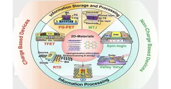
Every gadget is expected to address difficulties related to ordinary registration in another manner. Every one of the four works at extremely low voltages and is portrayed as having low spillage, rather than the regular metal-oxide semiconductor field-impact semiconductors (MOSFETs) found in cell phones that channel power in any event when switched off. The new devices, on the other hand, are based on processing steps that are similar to those used to make MOSFETs. As a result, they could be made on a large scale using semiconductor manufacturing processes that are already standard in the industry.
According to Banerjee, the spin-based field-effect transistor, or spin-FET, which makes use of the electrons’ magnetic moment, or spin, to power the device, is the information-processing device that looks most promising of the two. In this situation, the materials have a place with the progress metal dichalcogenide gathering of mixtures, which depend on changing metals.
“The promise of energy-efficient high-performance computing and storage is made possible by the new gadgets, thanks to the special features of 2D materials.”
Arnab Pal, who recently received his doctorate, is the lead author.
Not at all like the twist FET, the charge-based field-impact semiconductor, or TFET, works by exploiting the quantum-mechanical nature of electrons. Electrons can tunnel through a thin electrical barrier rather than flow over it in a conventional transistor thanks to a phenomenon known as wave-function penetration. Additionally, TFETs can function at lower voltages, using less power and producing less heat. TFETs made with 2D materials perform better as a result of their more slender and more controllable electronic burrowing hindrance, which both upgrades the electron stream and permits the gadget to perform with more noteworthy accuracy.
A device’s hard drive must be programmed so that storage is maintained even when power is off in order for data to be stored securely. Pal stated, “You have the source (electrons) and the drain (where the electrons are collected), and then the channel between them, which controls the flow of those carriers,” in order to accomplish this with a conventional MOSFET. The electrons can either not cross the channel, which is the off state, or they can cross it, which is the on state, because the channel is very conductive. In a typical n-type device, flow can only be produced by applying a positive gate bias—a voltage—that draws negatively charged electrons from the source across the channel.
In the meantime, the charge-based floating-gate field-effect transistor (FG-FET) information storage device functions in a manner that is comparable to that of a MOSFET, but it has two gate electrodes instead of just one. The additional cathode is known as a drifting entryway. The floating gate of a MOSFET does not incur any additional costs when it is unprogrammed. However, a very strong voltage is applied to the gate during any programming operation, pulling many carriers (electrons) from the channel and depositing them there, where they become trapped. The device is programmed to be off because it is difficult to turn on due to the accumulation of negative gate charges.
The researchers claim that this approach faces difficulties. One of them, Buddy said, is “pulling a ton of charge to the drifting entryway, which requires a great deal of force.” Banerjee continued, “Those electrons have to tunnel through a dielectric layer in order for them to arrive at the floating gate to program the device.” Additionally, once there, they may leak back, posing a charge retention issue.
Next-generation information processing and storage technologies may be made possible by a collection of charge- and non-charge-based devices made with two-dimensional materials.
Another issue is that the stored charges on the devices interact with one another, affecting the device next to it, when a large number of FG-FETs are placed close together—Pal stated, “We want to put as many on the chip as possible to, for example, increase the capacity of a thumb drive.” When ultra-thin 2D materials are used, this interaction is reduced while device control is increased, resulting in high performance even when there are more devices on the chip.
Utilizing magnetic tunnel junctions (MTJs), which make use of electron spin to store data, is yet another strategy for storing information. A MTJ comprises two attractive layers isolated by a dainty protective layer. The device’s resistance is determined by the layers’ relative orientation of their magnetic moments. However, just like FG-FETs, MTJs face difficulties in terms of stability, scalability, and power consumption. Again, by reducing interactions between adjacent MTJs, ultra-thin 2D materials provide a potential solution for this problem, making high-density, efficient data storage possible.
While gadgets made with 2D materials can yield enhancements as far as energy and region proficiency over those made with regular materials, unprecedented upgrades can be accomplished simply by changing the figuring engineering. Quantum computing, a radical new architecture, is here. Quantum computing makes use of the quantum superposition of quantum bits, or qubits, to generate parallel computations, resulting in significant speed and efficiency enhancements for specific computing tasks.
The more recent spin-, valley-, and spin-valley qubits, as well as the more conventional charge-based qubits, can be efficiently designed thanks to the distinctive structural and electromagnetic properties of two-dimensional materials.
In a twist qubit, the property of the state (on or off) is characterized by the electron twist, or quantum state, of the qubit, which is in every case either turn up or turn down. To change the state of the qubit and support qubit operation, the spin is flipped from up to down or vice versa.
The valley qubit works in a slightly different way. The electron’s momentum, rather than its spin, determines its state. The adjustment of the electron energy means a change in the qubit state, assisting with acknowledging qubit activity.
At long last, the properties of 2D materials can likewise help in understanding the third sort of qubit, the twist valley qubit, whose conditions are characterized by both the force and the twist of the electrons. Spin-valley qubits are thought to be more resistant to decoherence because they connect these two degrees of freedom. This means that they can carry out longer and more complex quantum computations before quantum entanglement is lost.
Pal stated, “The emerging devices, enabled by the unique properties of 2D materials, offer the promise of energy-efficient high-performance computing and storage,” “enabling beyond Moore integration and sparking new explorations in solid-state physics and their applications,” and “offering the promise of energy-efficient high-performance computing and storage.”
More information: Arnab Pal et al, Quantum‐Engineered Devices Based on 2D Materials for Next‐Generation Information Processing and Storage, Advanced Materials (2022). DOI: 10.1002/adma.202109894


