The University of Tokyo team, under the direction of Professor Naoya Shibata, worked with Sony Group Corporation to successfully observe up close a two-dimensional electron gas that had gathered at the semiconductor interface.
Highly effective light-emitting diodes (LEDs) and laser diodes (LDs) are made from GaN-based components. These are anticipated to be used as next-generation high-frequency devices for communication as well as power devices for power conversion due to their high dielectric breakdown strength and saturated electron velocity.
A layer of accumulated electrons known as a two-dimensional electron gas is produced at the semiconductor interface, specifically by high-electron-mobility transistors (HEMTs). The high electron mobility of this layer makes HEMTs ideal for high-frequency operation.
The performance of semiconductor devices depends critically on the characteristics of this two-dimensional electron gas, which have been estimated through indirect experiments or theoretical calculations. It is difficult to directly observe and confirm these phenomena, though.
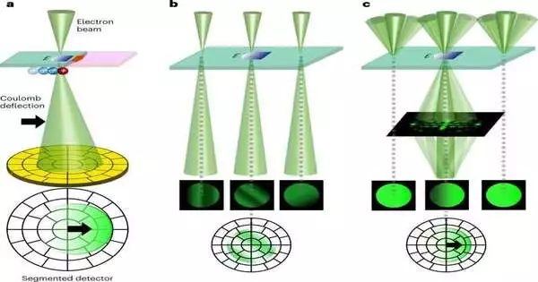
In this study, the research team used a newly developed tilt-scan system, magnetic-field-free atomic resolution STEM (MARS), and an ultrahigh-sensitivity, high-speed division-type detector to directly observe the two-dimensional electron gas that accumulated at the gallium nitride/aluminum indium nitride (GaN/AlInN) heterointerface.
The team used the atomic resolution differential phase contrast (DPC) method, an electromagnetic field observation method developed by Professor Shibata and others, to make observations. The two-dimensional electron gas that accumulated in the several nanometer-wide region of the semiconductor interface was successfully visualized and quantified. These developments allowed for two-dimensional electron gas control and are anticipated to boost transistor performance even more.
The research’s findings have led to advancements in semiconductor device interface analysis and control, enabling the creation of high-performance, high-frequency, and high-power devices that regulate two-dimensional electron gas. This has also produced cutting-edge measurement technologies that have the potential to make significant contributions to the study and creation of cutting-edge components and apparatus.
The study has been published in the journal Nature Nanotechnology.
More information: Satoko Toyama et al, Real-space observation of a two-dimensional electron gas at semiconductor heterointerfaces, Nature Nanotechnology (2023). DOI: 10.1038/s41565-023-01349-8


