Solar cells that convert the sun’s energy into electricity will play a vital role in the world’s future energy supply as climate change and its implications become more apparent.
To avoid imperfections in their crystal structure that impair functionality, common semiconductor materials for solar cells, such as silicon, must be produced using a costly technique. Metal-halide perovskite semiconductors, on the other hand, are emerging as a less expensive, alternative material class with good and tunable functionality as well as processing ease.
Researchers provide a road map for organic-inorganic hybrid perovskite semiconductors and devices in APL Materials, published by AIP Publishing.
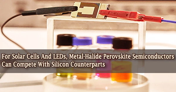
To make the required film, perovskite semiconductors can be treated from solution, and a semiconductor ink can be coated or simply painted over surfaces. This could be used in semiconductor devices like solar cells and light-emitting diodes.
“For many years, solution-processed semiconductors were viewed as unable to deliver the same functionality as specially grown crystalline semiconductors,” said Lukas Schmidt-Mende, a co-author from the University of Konstanz in Germany.
“The reason behind this thinking was that simple solution processing will inherently lead to a relatively high number of defects within the formed crystal structure, which can negatively affect its functionality.”
Organic-inorganic hybrid perovskites turn out to be exceedingly defect-tolerant. Defects created during processing have little impact on device operation, and hybrid perovskites are enabling efficient solution-processed devices for the first time.
“We can simply change the chemical composition of the perovskite to tune its bandgap, which allows us to change the absorption profile,” said Schmidt-Mende. “This can be used to prepare light-emitting diodes at different wavelengths or to tune the perovskite material for tandem solar cells to optimize the absorption profile.”
Although the stability of perovskite devices has increased dramatically during the past few years, we still do not understand and have not overcome all of its degradation mechanisms.
Schmidt-Mende
High defect tolerance, however, “came as a surprise that needs to be better understood,” he said. “Understanding the details will help to further optimize the material, perhaps to find other similar efficient alternatives and give us the chance to improve applications based on perovskite semiconductors.”
Perovskite devices now have two key limitations, according to the group.
To begin with, all of the most efficient devices include hazardous lead, and efforts to replace it with less toxic components have only been partially effective thus far. Second, compared to silicon devices, perovskite devices have a shorter life period.
“Although the stability of perovskite devices has increased dramatically during the past few years, we still do not understand and have not overcome all of its degradation mechanisms,” said Schmidt-Mende.
Many researchers are working on solar cells, and because perovskites have the ability to tune the bandgap, they are appealing for tandem applications where they can be paired with a well-established silicon solar cell.
“Other applications are light-emitting diodes, where the color of the light emitted can be tuned by adjusting the chemical composition of the perovskite,” Schmidt-Mende said. “As for other semiconductors, the list of possible applications is long, and we are just beginning to understand this material and its potential.”


