Several times more grounded than steel, graphene has been hailed as a material representing things to come since its disclosure in 2004. The ultrathin carbon material is a staggeringly solid electrical and thermal channel, making it an ideal fix to upgrade semiconductor chips tracked down in numerous electrical gadgets.
Yet, while graphene-based research has been optimized, the nanomaterial has hit detours: specifically, makers have not had the option to make huge, mechanically pertinent measures of the material. A new exam from the lab of Nai-Chang Yeh, the Thomas W. Hogan Teacher of Material Science, is reviving the graphene frenzy.
In two new examinations, the analysts show that graphene can enormously further develop electrical circuits expected for wearable and adaptable gadgets, for example, savvy wellbeing patches, bendable cell phones, caps, huge collapsing show screens, and then some.
In one review, published in ACS Applied Materials and Connection Points, the analysts developed graphene straightforwardly onto slim two-layered copper lines usually utilized in gadgets. The outcomes showed that the graphene further developed the lines’ leading properties as well as shielded the copper-based structures from common mileage. For example, they showed that graphene-covered copper designs could be collapsed multiple times without harm when contrasted with the first copper structures, which began breaking after 20,000 folds. The results show that graphene can assist in making adaptable gadgets with longer lifetimes.
The subsequent review, published in ACS Applied Nano Materials, showed that gold covered in graphene could more readily endure the perspiration of an individual’s body and hence would improve implantable biosensors. Gold is a common material used in the development of implantable biosensors or smart patches—nanoscale devices for diagnosing various diseases.Graphene dials back the rate at which the gold is eroded.
The two examinations, notwithstanding a third report in ACS Applied Materials and Connection Points showing that graphene can safeguard electrical circuits created through inkjet printers, utilized the Yeh group’s novel strategy for developing graphene. In 2015, Yeh and her partners, including senior examination researcher David Boyd, declared that they had sorted out a superior, more savvy, and harmless to the ecosystem method for developing graphene on materials. The method can be used to create great graphene sheets only a single iota thick at room temperature in about 15 minutes.This is rather than different strategies that require a lot higher temperatures, cruel synthetics, and require a few hours to finish.
“Adaptable and wearable gadgets can be made of delicate materials like polymers that can’t support high temperatures,” says Chen-Hsuan (Steve) Lu, a Caltech graduate understudy and lead creator of the three examinations. “Our strategy permits us to develop graphene straightforwardly on the substrates at a low temperature, forestalling any harm to delicate materials.”
Yeh adds that their graphene-development strategy, which can be increased for modern necessities, is viable with a large group of different applications, notwithstanding adaptable and wearable gadgets.
“Our strategy is profoundly viable with a wide range of substrates, going from small, nanostructured metals, to semiconducting materials, to even plastics. “Since we don’t need high temperatures, this strategy can be used on various substrates for some applications,” she says.
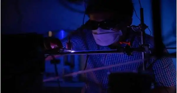
Pink plasma
The group’s strategy for developing sheets of graphene is carried out in their cellar lab. A beam of plasma, which shines pink, is utilized to enact a gas of hydrogen and methane particles and separate them into more modest pieces. The example, for example, a two-layered copper line, is then drenched in the plasma, and the carbon from the gas gets kept onto the surface in slim sheets that are one iota thick. The last surface with graphene will seem shinier.
“Since the example is drenched in the plasma without the need for dynamic warming up to around 1,000 degrees Celsius by a hot heater, which is the situation with different techniques, much lower-temperature development becomes doable,” Lu says.
For the review that tried graphene’s capacity to upgrade the adaptability of gadgets, the group cooperated with the Materials and Compound Exploration Labs at the Taiwanese association called Modern Innovation Exploration Foundation (ITRI). The Caltech group created graphene-covered copper structures that mimic what might be used in adaptable gadgets and then had their collaborators at ITRI crease them; the organization has the equipment required to overlap the designs numerous times more than once.”I attempted but couldn’t remain there and crease the materials this long myself,” Lu jokes.
“The ITRI has been playing a significant part in spanning lab examinations to modern creations in Taiwan over many years. “The most notable model among many side project organizations from ITRI is the Taiwan Semiconductor Assembling Organization (TSMC), as of now the world’s biggest and driving semiconductor foundry,” says Yeh, who has recently gone to Taiwan to visit her partners at ITRI.
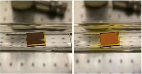
After a substrate is covered with graphene, it seems shinier (ok). Credit: Caltech
In this equivalent review, the analysts likewise showed that graphene could further develop the copper designs’ compound strength and electrical conductivity, notwithstanding their primary adaptability. “We put only two nuclear layers of graphene on top of these slim copper lines and saw that they were perfectly unaltered after a while,” Yeh says.
The subsequent review tested whether graphene could safeguard the strength of gold designs utilized in implantable biosensors. The analysts developed graphene on gold and afterward presented the material to saline arrangements that copy sweat. The results showed that the graphene-covered structure stayed in one piece under conditions identical to around one month at typical human internal heat levels, significantly longer than whatever is conceivable with gold alone.
“I didn’t know about graphene’s maximum capacity when I initially began working with it,” Lu says. “I didn’t know about graphene’s maximum capacity when I initially began working with it,” Lu says. However, at that point, I understood how it tends to be utilized paired with different materials for so many countless applications. My flat mate [co-creator Kuang Ming (Allen) Shang] and I were having a boba tea when we understood we could test whether graphene could shield gold from the destructive impacts of sweat. Lu says that his favorite Taiwanese beverage, boba tea, assists in moving him with novel thoughts.
What is next for graphene?
While graphene has taken longer than expected to make its way into devices, its future looks bright.Notwithstanding the utilization of graphene in wearable and adaptable gadgets, Yeh is analyzing graphene’s likely in everything from energy research and optical correspondences to harmless to the ecosystem batteries, and that’s just the beginning.
Graphene is also key, she says, to the developing field of nanoelectronics, which plans to make more modest forms of the gadgets broadly utilized today. Graphene can be utilized in combination with silicon to recoil gadgets down to increasingly small sizes.
Graphene, when joined with different materials, can make our nanotechnologies more modest and quicker. It prompts lower heat dispersion and energy utilization. In our lab, we use graphene for so many countless things. It’s energizing, “she says.
More information: Chen-Hsuan Lu et al, Polymer-Compatible Low-Temperature Plasma-Enhanced Chemical Vapor Deposition of Graphene on Electroplated Cu for Flexible Hybrid Electronics, ACS Applied Materials & Interfaces (2021). DOI: 10.1021/acsami.1c11510
Chen-Hsuan Lu et al, Graphene on Nanoscale-Thick Au Films: Implications for Anticorrosion in Smart Wearable Electronics, ACS Applied Nano Materials (2022). DOI: 10.1021/acsanm.2c00401
Journal information: ACS Applied Materials and Interfaces


