The semiconductor business today is attempting to answer a triple order: expanding processing power, diminishing chip measures, and overseeing power in thickly stuffed circuits.
To satisfy these needs, the business should look beyond silicon to deliver gadgets proper for the developing job of figuring.
While it is far-fetched to leave the workhorse material in the near or far future, the innovation area will require imaginative improvements in chip materials and structures to create gadgets fitting for the developing job of registering.
One of the greatest inadequacies of silicon is that it must be made so flimsy in light of the fact that its material properties are, in a general sense, restricted to three aspects [3D]. Hence, two-layered [2D] semiconductors—so slight as to have basically no level—have turned into an object important to researchers, designers, and microelectronics makers.
More slender chip parts would give more noteworthy control and accuracy over the progression of power in a gadget while bringing down how much energy is expected to drive it. A 2D semiconductor would likewise add to keeping the surface region of a chip to a base, lying in a meager film on a supporting silicon gadget.
“Semiconductor manufacturing is a large-scale manufacturing process. You won’t have a viable material unless you can build it on industrial-scale wafers. The lower the price, the more chips you can produce in a batch. To ensure performance, however, the material must also be pure. This is why silicon is so common—it can be produced in enormous quantities without sacrificing purity.”
Deep Jariwala, Associate Professor Distinguished Scholar in the Department of Electrical and Systems Engineering (ESE),
In any case, as of not long ago, endeavors to make such a material had been fruitless.
Certain 2D semiconductors have performed well all alone; however, they expected such high temperatures to destroy the basic silicon chip. Others could be saved at silicon-viable temperatures; however, their electronic properties—energy use, speed, and accuracy—were inadequate. Some fit the bill for temperature and execution yet couldn’t be developed to the essential immaculateness at industry-standard sizes.
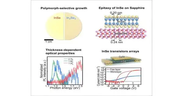
Presently, specialists at the College of Pennsylvania School of Designing and Applied Science have grown a high-performing 2D semiconductor into a standard, modern-scale wafer. What’s more, the semiconductor material, indium selenide (InSe), can be stored at temperatures sufficiently low to be incorporated into a silicon chip.
Profound Jariwala, an academic administrator, and Peter and Susanne Armstrong, recognized researchers in the Branch of Electrical and Frameworks Designing (ESE), and Seunguk Tune, a postdoctoral individual in ESE, drove the review, which was distributed late in the issue.
“Semiconductor production is a modern-scale fabricating process,” says Jariwala. “You won’t have practical material except if you can deliver it on modern-scale wafers. The more chips you can make in a group, the lower the cost. However, the material must also be unadulterated to guarantee execution. Therefore, silicon is so pervasive—you can make it in enormous amounts without forfeiting immaculateness.”
InSe has long been guaranteed as a 2D material for cutting-edge registration chips since it conveys electrical charge particularly well. In any case, creating enormous enough movies of InSe has demonstrated precariousness in light of the fact that the science of indium and selenium will in general consolidate to a couple sub-atomic extents, taking on compound designs with differing proportions of every component and hence undermining its virtue.
The group’s prosperity relied on Melody’s use of a development procedure that conquered the characteristics of InSe’s nuclear construction.
“For the reasons of high-level figuring innovation, the compound design of 2D InSe should be precisely 50:50 between the two components. The subsequent material necessity is a uniform compound design over an enormous region to work,” says Tune.
The group accomplished this noteworthy virtue by utilizing a development procedure called “vertical metal-natural substance fume testimony” (MOCVD). Past examinations have endeavored to present indium and selenium in equivalent amounts and simultaneously. Tune illustrated, nonetheless, that this strategy was the wellspring of unfortunate compound designs in the material, delivering particles with shifting proportions of every component. MOCVD, paradoxically, works by sending the indium in a consistent stream while presenting the selenium in beats.
“By beating, you give the indium and selenium time to consolidate. At the times between beats, you deny the climate of selenium, which keeps the proportion from getting excessively high. The advantage of the beat is the interruption. That is the way we get a uniform 50:50 proportion across our whole regular wafer,” says Melody.
Notwithstanding compound immaculateness, the group was likewise ready to control and adjust the heading of precious stones in the material, improving the nature of their semiconductor considerably further by giving a consistent climate to electron transport.
“The two most significant material characteristics in a semiconductor are compound virtue and glasslike request. The main modern quality is versatility. This material really takes a look at each case,” says Jariwala.
More information: Seunguk Song et al, Wafer-scale growth of two-dimensional, phase-pure InSe, Matter (2023). DOI: 10.1016/j.matt.2023.07.012


