The world’s smallest LED (light-emitting diode) has been developed by Singaporean researchers, making it possible to transform existing mobile phone cameras into high-resolution microscopes. The new LED, which was used to construct the world’s smallest holographic microscope and was smaller than the wavelength of light, paved the way for existing cameras in everyday devices like mobile phones to be transformed into microscopes by only modifying the silicon chip and software. This innovation likewise addresses a huge step in the right direction in the scaling down of diagnostics for indoor ranchers and reasonable farming.
In addition, the researchers created a ground-breaking neural networking algorithm that can reconstruct objects measured by the holographic microscope. This makes it possible to examine microscopic objects like cells and bacteria more thoroughly without using bulky conventional microscopes or additional optics. The development of a powerful on-chip emitter that is smaller than a micrometer, which has long been a challenge in the field, is also paved over by the research, opening the door to a significant advancement in photonics.
The light in most photonic chips originates from off-chip sources, which generally leads to low energy proficiency and, on a very basic level, restricts the versatility of these chips. On-chip emitters made of rare-earth-doped glass, Ge-on-Si, and heterogeneously integrated III-V materials have been developed as a solution to this problem. Although emitters based on these materials have demonstrated promising device performance, it is still challenging to incorporate their fabrication procedures into conventional complementary metal-oxide-semiconductor (CMOS) platforms.
“Our novel LED has several potential uses outside lensless holography, which it has tremendous potential for. Our LED would be perfect for near-field microscopy and implanted CMOS devices since its wavelength is inside the minimal absorption window of biological tissues, together with its high intensity and nanoscale emission area.”
Rajeev Ram, principal investigator at SMART CAMP and DiSTAP, Professor of Electrical Engineering at MIT .
While silicon (Si) has shown potential as an up-and-comer material for nanoscale and exclusively controllable producers, Si producers experience the ill effects of low quantum effectiveness in light of the roundabout bandgap, and this principal drawback, joined with the limits set by the accessible materials and devices, has obstructed the acknowledgment of a little local Si producer in CMOS.
SMART researchers described their development of the smallest reported Si emitter with a light intensity comparable to that of state-of-the-art Si emitters with much larger emission areas in a recent Nature Communications paper titled “A sub-wavelength Si LED integrated in a CMOS platform.” In a paper titled “Simultaneous spectral recovery and CMOS micro-LED holography with an untrained deep neural network,” which was recently published in the journal Optica, SMART researchers also unveiled their construction of a novel, untrained deep neural network architecture that is capable of reconstructing images from a holographic microscope.
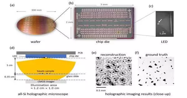
The original Drove created by Brilliant specialists is a CMOS-coordinated sub-frequency scale Drove at room temperature, displaying high spatial force (102 48 mW/cm2) and having the littlest emanation region (0.09 0.04 m2) among all known Si producers in logical writing. The researchers then integrated this LED into an in-line, centimeter-scale, all-silicon holographic microscope that did not require a lens or pinhole, which is an essential component of the field known as lensless holography. This was done in order to demonstrate a potential practical application.
An illustration of how the LED, holographic microscope, and neural network are used to reconstruct an image Credit: Computational reconstruction of the imaged object is a common obstacle in lensless holography, as demonstrated by the Singapore-MIT Alliance for Research and Technology (SMART). For accurate reconstruction, traditional reconstruction techniques are sensitive to variables that are difficult to control, such as optical aberrations, the presence of noise, and the twin image problem.
The exploration group likewise fostered a profound brain network design to work on the nature of picture recreation. This novel, untrained deep neural network takes into account the source’s extensive spectral bandwidth and incorporates total variation regularization for enhanced contrast.
Not at all like conventional strategies for computational reproduction that require preparing information, this brain network disposes of the requirement for preparing by installing a material science model inside the calculation. The neutral network offers blind source spectrum recovery from a single diffracted intensity pattern in addition to holographic image reconstruction, a ground-breaking departure from all previous supervised learning methods.
The undeveloped brain network shown in this study permits scientists to utilize novel light sources without earlier information on the source range or shaft profile; for example, the novel and least realized Si Drove depicted above was manufactured by means of a completely unmodified mass CMOS microelectronics.
Other computational imaging applications, such as a compact microscope for live-cell tracking or spectroscopic imaging of biological tissues like living plants, could benefit from this synergistic combination of the neural network and CMOS micro-LEDs. Additionally, this work demonstrates the viability of future on-chip imaging systems. Particle tracking, environmental monitoring, biological sample imaging, and metrology are just a few of the many uses for in-line holography microscopes. These LEDs could also be used to create programmable coherent illumination for future, more complex systems by being arranged in CMOS.
Iksung Kang, lead creator of the Optica paper and exploration right hand at MIT at the hour of this examination, said, “Our advancement addresses a proof of idea that could be immensely significant for various applications requiring the utilization of miniature LEDs. For instance, this LED could be incorporated into an array to provide the higher levels of illumination required for applications on a larger scale. In addition, this can be accomplished without increasing the system’s complexity, cost, or form factor due to the microelectronics CMOS processes’ low cost and scalability. This empowers us to change, no sweat, a cell phone camera into a holographic magnifying lens of this sort. By making use of the electronics that are already available, control electronics and even the imager could be incorporated into the same chip, creating an all-in-one micro-LED that could revolutionize the industry.”
“On top of its enormous potential in lensless holography, our new Driven has a large number of other potential applications.” Our LED could be ideal for bio-imaging and bio-sensing applications, including near-field microscopy and implantable CMOS devices,” said Rajeev Ram, principal investigator at SMART CAMP and DiSTAP, Professor of Electrical Engineering at MIT and co-author of both papers. “Its wavelength is within the minimum absorption window of biological tissues, along with its high intensity and nanoscale emission area.” This LED could also be used in on-chip communication, NIR proximity sensing, and on-wafer photonics testing if it is integrated with on-chip photodetectors.”
More information: Zheng Li et al, A sub-wavelength Si LED integrated in a CMOS platform, Nature Communications (2023). DOI: 10.1038/s41467-023-36639-1
Iksung Kang et al, Simultaneous spectral recovery and CMOS micro-LED holography with an untrained deep neural network, Optica (2022). DOI: 10.1364/OPTICA.470712


