Two-layered (2D) semiconductors are semiconducting materials with thicknesses on the nuclear scale that have uncommon electronic properties. Later on, these materials could possibly supplant silicon in the improvement of various electronic and optoelectronic gadgets.
In spite of their benefits, the utilization of 2D semiconductors has so far been restricted, somewhat because of their low transporter portability at room temperature. This is brought about by areas of strength for phonons (i.e., quasiparticles related to aggregate nuclear vibrations) in the materials’ grids.
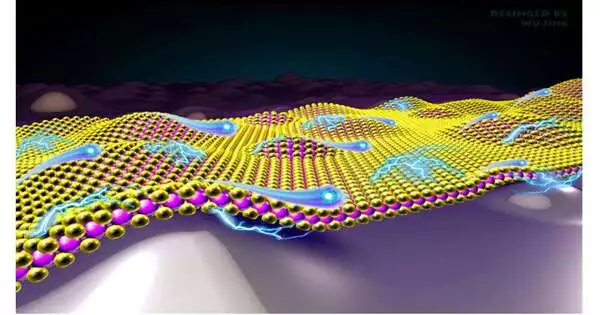
Scientists at the Agency for Science, Technology, and Research (A*STAR) in Singapore and the Hong Kong Polytechnic University in Hong Kong, China have as of late contrived a plan system that could assist with beating this limit, further developing the transporter versatility of 2D materials. Their proposed approach, framed in a paper distributed in Nature Electronics, involves the presentation of grid bends in a 2D material, utilizing swell substrates.
“We simply placed 2D materials on substrates with bulged morphologies, generating ripples in the material that leads to lattice distortion.” “Typically, lattice distortions are expected to reduce carrier mobility. However, we show that such lattice distortions produce more electric polarization, which not only renormalizes phonon frequency to effectively suppress scattering between electrons and phonons, but also increases the intrinsic dielectric constant to further screen polar phonon scattering.”
Dr. Ming Yang and Dr. Jing Wu.
“Our paper was roused by the high transporter portability seen in 2D TMDs on substrates with high surface harshness by Tao Liu et al. back in 2019,” Dr. Ming Yang and Dr. Jing Wu. Two of the analysts who did the review told TechXplore. However, the noticeable portability improvement was only attributed to strain effects, and the underlying system remains unknown.To this end, we dug further to unwind the basic physical science liable for such a huge upgrade in portability and show grid designing as a viable system to make elite-execution electronic gadgets at room temperature.
Most regular systems for further developing the transporter versatility of 2D semiconductors depend on achieving ideal grid structures. The system proposed by Yang, Wu, and their partners, then again, only involves the presentation of lump substrates, which induce swells in a 2D semiconductor and stifle the dispersion of phonons.
Yang and Wu made sense of it by saying, “We just put 2D materials on substrates with swell morphologies, making swells in the material that prompt grid bending.” “Commonly, grid bends are scheduled to influence transporter versatility unfavorably.” In any case, we show that such grid bends make a bigger electric polarization, which can not just renormalize the recurrence of phonons to really stifle dispersing among electrons and phonons, but in addition improve the natural dielectric steady to further screen the polar phonon dissipation. “
Contrasted with other existing methodologies for expanding transporter portability in 2D semiconductors, the system proposed by these analysts is both basic and savvy. As a feature of their review, the group tried it on 2D molybdenum disulfide (MoS2) and found that it brought about room temperature transporter portability of roughly 900 cm2 V1 s1, which surpasses the anticipated phonon-restricted versatility of level MoS2 (going somewhere in the range of 200 and 410 cm2 V1 s1).
“The noticed portability upgrade and the basic system of such high transporter versatility in undulated MoS2, which surpasses the anticipated phonon-restricted versatility in level MoS2, is especially vital,” Yang and Wu said. “Such high transporter versatility can prepare for low-fueled gadgets and is a significant boundary for most applications going from field-impact semiconductors to photodetectors and then some.”
The review conducted by this group of analysts features the immense capability of grid designing systems to improve the exhibition of gadgets and thermoelectric gadgets at room temperature. Later on, their strategy could be utilized to make more effective gadgets in view of 2D semiconductors. Also, it might actually promote the advancement of other planning systems in view of grid designing.
“In our next examinations, we plan to efficiently make undulated/swell substrates to limit fluctuation, as well as to concentrate on the connections between lumps,” Yang and Wu added.
More information: Hong Kuan Ng et al, Improving carrier mobility in two-dimensional semiconductors with rippled materials, Nature Electronics (2022). DOI: 10.1038/s41928-022-00777-z


