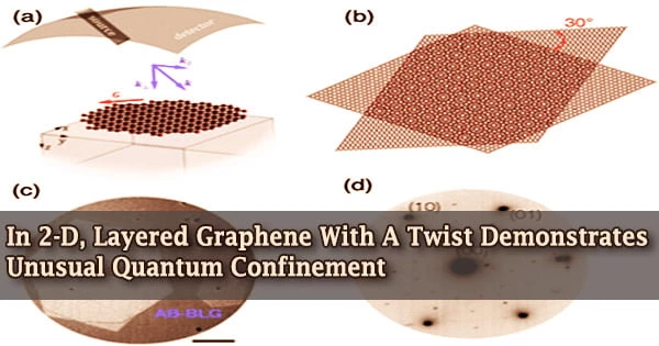
Scientists have discovered electrical and optical interlayer resonances in two different configurations of bilayer graphene, a two-dimensional (2-D), an atom-thin form of carbon. Electrons bounce back and forth between the two atomic planes in the 2-D interface at the same frequency in these resonant states.
They discovered that rotating one of the graphene layers by 30 degrees relative to the other, rather than stacking the layers squarely on top of one other, causes the resonance to move to lower energy.
They extrapolated from this data, which was recently published in Physical Review Letters, that the distance between the two layers in the twisted arrangement rose dramatically when compared to the stacked form.
Interlayer interactions alter when this distance changes, influencing how electrons travel in the bilayer system. Understanding the mobility of electrons could aid in the development of future quantum technologies for more powerful computation and secure communication.
“Today’s computer chips are based on our knowledge of how electrons move in semiconductors, specifically silicon,” said first and co-corresponding author Zhongwei Dai, a postdoc in the Interface Science and Catalysis Group at the Center for Functional Nanomaterials (CFN) at the U.S. Department of Energy (DOE)’s Brookhaven National Laboratory.
“But the physical properties of silicon are reaching a physical limit in terms of how small transistors can be made and how many can fit on a chip. If we can understand how electrons move at the small scale of a few nanometers in the reduced dimensions of 2-D materials, we may be able to unlock another way to utilize electrons for quantum information science.”
The scale of a material system is comparable to the wavelength of electrons at a few nanometers, or billionths of a meter. The electrical and optical properties of a material change when electrons are confined in a space with dimensions equal to their wavelength.
Rather than classical mechanical motion, in which electrons flow through a material and are scattered by random flaws, these quantum confinement phenomena are the result of quantum mechanical wave-like motion.
Today’s computer chips are based on our knowledge of how electrons move in semiconductors, specifically silicon. But the physical properties of silicon are reaching a physical limit in terms of how small transistors can be made and how many can fit on a chip. If we can understand how electrons move at the small scale of a few nanometers in the reduced dimensions of 2-D materials, we may be able to unlock another way to utilize electrons for quantum information science.
Zhongwei Dai
The scientists used two separate probes: electrons and photons, to examine quantum confinement phenomena using a basic material model called graphene (particles of light). They employed an unique substrate onto which the graphene could be transported to test both electrical and optical resonances. Jurek Sadowski, co-corresponding author and member of the CFN Interface Science and Catalysis Group, has previously designed this substrate for the Quantum Material Press (QPress).
The QPress is an automated instrument for the synthesis, processing, and characterization of layered 2-D materials that is being developed at the CFN Materials Synthesis and Characterization Facility. On a silicon dioxide substrate several hundred nanometers thick, scientists exfoliate 2-D material “flakes” from 3-D parent crystals (e.g., graphene from graphite).
However, because this substrate is insulating, electron-based probing techniques are ineffective. As a result, Sadowski and CFN scientist Chang-Yong Nam, as well as Stony Brook University graduate student Ashwanth Subramanian, created a conductive layer of titanium oxide on the silicon dioxide substrate that was only three nanometers thick.
“This layer is transparent enough for optical characterization and determination of the thickness of exfoliated flakes and stacked monolayers while conductive enough for electron microscopy or synchrotron-based spectroscopy techniques,” explained Sadowski.
The University of Pennsylvania’s Charlie Johnson Group The graphene was grown on metal foils and placed onto the titanium oxide/silicon dioxide substrate by Rebecca W. Bushnell Professor of Physics and Astronomy Charlie Johnson, postdoc Qicheng Zhang, and former postdoc Zhaoli Gao (now an assistant professor at the Chinese University of Hong Kong).
All three domains (single layer, stacked, and twisted) are present when graphene is formed in this manner. Then, using a low-energy electron microscope (LEEM), Dai and Sadowski devised and carried out tests in which they fired electrons into the material and recorded the reflected electrons.
They also fired photons into the material using a laser-based optical microscope with a spectrometer and examined the spectrum of light scattered back. This confocal Raman microscope is part of the QPress cataloger, which can locate the locations of sample areas of interest using image-analysis software and the QPress cataloger.
“The QPress Raman microscope enabled us to quickly identify the target sample area, accelerating our research,” said Dai.
The distance between layers in the twisted graphene form rose by around 6% compared to the non-twisted configuration, according to their findings. Theoretical calculations at the University of New Hampshire confirmed the twisted configuration’s unique resonant electrical characteristics.
“Devices made out of rotated graphene may have very interesting and unexpected properties because of the increased interlayer spacing in which electrons can move,” said Sadowski.
The scientists will then use the twisted graphene to create devices. The team will also expand on previous work by CFN staff scientist Samuel Tenney and CFN postdocs Calley Eads and Nikhil Tiwale to investigate how different materials affect the layered structure’s electrical and optical capabilities.
“In this initial research, we picked the simplest 2-D material system we can synthesize and control to understand how electrons behave,” said Dai. “We plan to continue these types of fundamental studies, hopefully shedding light on how to manipulate materials for quantum computing and communications.”
The DOE Office of Science funded this study, which made use of the CFN and the National Synchrotron Light Source II (NSLS-II), both DOE Office of Science User Facilities in Brookhaven.
The LEEM microscope is part of the x-ray photoemission electron microscopy (XPEEM)/LEEM endstation of the Electron Spectro-Microscopy beamline at NSLS-II; the CFN operates this endstation through a partner user agreement with NSLS-II. The National Science Foundation, the Research Grant Council of the Hong Kong Special Administrative Region, and the Chinese University of Hong Kong are the other financial bodies.


