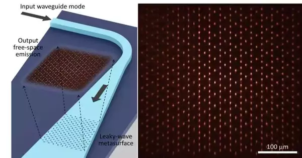
“Leaky-wave metasurfaces,” a new class of integrated photonic devices created by Columbia Engineering, are capable of converting light initially contained in an optical waveguide into any arbitrary optical pattern in free space. As a world record, these devices are the first to simultaneously control all four optical degrees of freedom—amplitude, phase, polarization ellipticity, and orientation.
The devices can be used to enhance optical displays, LIDAR (light detection and ranging), optical communications, and quantum optics due to their transparency, compatibility, and thinness.
“We are excited to find an elegant solution for interfacing free-space optics and integrated photonics,” said Nanfang Yu, an associate professor of applied physics and applied mathematics who is leading research on nanophotonic devices. “These two platforms have traditionally been studied by investigators from different subfields of optics and have led to commercial products addressing completely different needs.”
“We are thrilled to have discovered an elegant solution for bridging free-space optics and integrated photonics—these two platforms have traditionally been studied by investigators from different subfields of optics and have resulted in commercial products addressing completely different needs,”
Nanfang Yu, associate professor of applied physics and applied mathematics.
“Our work points to new ways to create hybrid systems that address many emerging applications such as quantum optics, optogenetics, sensor networks, inter-chip communications, and holographic displays.” These hybrid systems use integrated photonics for optical data processing and free-space optics for shaping the wavefront of light.
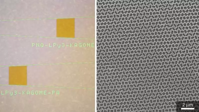
Left: A picture of two leaky-wave metasurfaces that can be used to create Kagome lattices. Right: A leaky-wave metasurface composed of nano-apertures etched into a polymer layer on top of a thin film of silicon nitride is depicted in a SEM image. Credit: Heqing Huang, Adam Overvig, and Nanfang Yu/Columbia Engineering
Bridging free-space optics and integrated photonics
The primary obstacle to integrating PICs with free-space optics is converting a straightforward waveguide mode contained within a waveguide—a thin chip ridge—into a broad free-space wave with a complex wavefront. The task at hand was met by Yu’s group by expanding on the “nonlocal metasurfaces” they had developed in the previous year and making them capable of controlling guided waves in addition to free-space light waves.
In particular, they extended the information waveguide mode by utilizing a waveguide tightening into a section waveguide mode — a sheet of light proliferating along the chip. ” Heqing Huang, a Ph.D. student in Yu’s lab and co-first author of the study that was published today in Nature Nanotechnology, stated, “We realized that the slab waveguide mode can be decomposed into two orthogonal standing waves—waves reminiscent of those produced by plucking a string.” The study was published today in Nature Nanotechnology.
“In order to independently control these two standing waves, we designed a “leaky-wave metasurface” consisting of two sets of rectangular apertures offset by a subwavelength.” “The outcome is that each standing wave is changed over into a surface outflow with free sufficiency and polarization; together, the two surface discharge parts converge into a solitary free-space wave with totally controllable sufficiency, stage, and polarization at each point over its wavefront.”
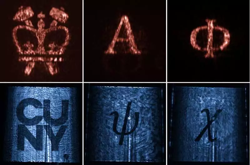
Left two numbers: At two distinct distances from the device’s surface, two holographic images are produced by a leaky-wave metasurface. Right four figures: At two orthogonal polarization states and at two distinct distances from the device surface, a single leaky-wave metasurface produced four distinct holographic images. Credit: Heqing Huang, Adam Overvig, and Nanfang Yu/Columbia Designing
From quantum optics to optical interchanges to holographic 3D showcases
Yu’s group tentatively exhibited different cracked wave metasurfaces that can change over a waveguide mode spreading along a waveguide with a cross-segment on the request for one frequency into free-space outflow with an originator wavefront over an area multiple times the frequency at the telecom frequency of 1.55 microns. These are some:
- A metalens with a leaky wave that creates a focal point in free space. Such a device will be ideal for establishing a free-space optical link between PIC chips with high capacity and low loss. An integrated optogenetic probe that uses focused beams to optically stimulate neurons far from the probe will also benefit from it.
- A leaky-wave optical-lattice generator capable of generating hundreds of focal spots that, in free space, form a Kagome lattice pattern. As a rule, the broken wave metasurface can deliver complex aperiodic and three-layered optical cross sections to trap cold iotas and particles. Researchers will be able to significantly reduce the complexity, volume, and cost of atomic-array-based quantum devices thanks to this capability, which will also make it possible for them to study exotic quantum optical phenomena or carry out quantum simulations that were previously difficult to achieve with other platforms. To simplify the optical system, the leaky-wave metasurface, for instance, could be directly integrated into the vacuum chamber, making portable quantum optics applications like atomic clocks a possibility.
- A cracked wave vortex-shaft generator that creates a bar with a wine tool forms a wavefront. Using light waves with shaped wavefronts for high-capacity intercommunication and PICs to process light-carried information, this could result in a free-space optical link between buildings.
- A hologram with leaky waves that can simultaneously move four different images: two at a distance in free space (also at two orthogonal polarization states) and two at the device plane (at two orthogonal polarization states). Holographic 3D displays and lighter, more comfortable augmented reality goggles could both benefit from this function.
At near-infrared wavelengths, Yu’s current demonstration is based on a straightforward polymer-silicon nitride material platform. Devices based on the more durable silicon nitride platform, which is compatible with foundry fabrication protocols and tolerant of high optical power operation, will be demonstrated next by his team. Additionally, they intend to demonstrate designs that operate at visible wavelengths with high output efficiency and are better suited to quantum optics and holographic displays.
More information: Andrea Alù, Leaky-wave metasurfaces for integrated photonics, Nature Nanotechnology (2023). DOI: 10.1038/s41565-023-01360-z. www.nature.com/articles/s41565-023-01360-z


