In materials science and applied physics, multicolored, miniaturized light-emitting device arrays offer a promising instrument for sensing, imaging, and computing. Conventional light-emitting diodes can produce a variety of emission colors, but the process may be constrained by device or material constraints.
A variety of highly multicolored light-emitting arrays with diverse colors on a single chip were developed by Vivian Wang and a research team in electrical engineering and materials science at the Lawrence Berkeley National Laboratory and the University of California, Berkeley, in a new report that was published in Science Advances. Electroluminescence from micro-dispersed materials of various colors and spectral shapes was produced by the array’s pulse-driven metal-oxide-semiconductor capacitors.
Using multiplexed electroluminescent arrays to demonstrate spectral imaging of samples in conjunction with a camera, the materials scientists and engineers combined compressive reconstruction algorithms to perform spectroscopic measurements in a compact setting.
Experimental design
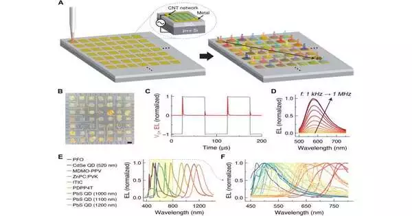
Kaleidoscopic light-radiating exhibits have flexible applications in the field, albeit the scope of varieties being used is deficient for business use. In this study, Wang and colleagues used arrays of electroluminescent, alternating current-driven metal oxide semiconductor capacitors to solve the issue. Before depositing the emitting materials, they lithographically defined the device electrodes. The statement of the emissive layer framed the last manufacturing step in these gadgets, and the group utilized microprinting strategies to effortlessly apportion different variety producers on a solitary chip to perform dynamic phantom estimations in a scaled-down climate.
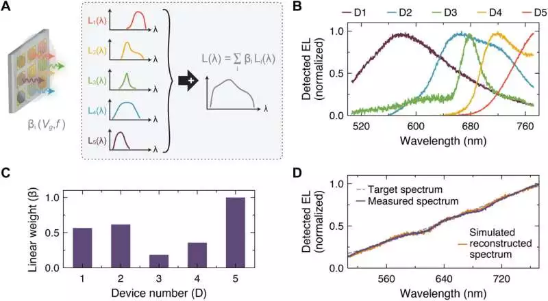
Design of any kind of EL spectrum. A) Schematic showing how an EL array can be used to generate any kind of EL spectrum B) Illustration of EL spectra and (C) relative loads of the relating spectra used to reproduce the objective range in (D). The desired target spectrum is depicted by the dashed gray curve. The spectrum that was experimentally measured using the five-device EL array is depicted by the purple curve. The calculated design spectrum is represented by the gold curve. Credit: Science Advances (2023). DOI: 10.1126/sciadv.adg1607
Electroluminescent device arrays with arbitrary spectra The team used metal-oxide-semiconductor capacitor devices to create multiplexed light sources by depositing emissive materials on top of silicon substrate-engineered capacitors. They applied a rotating current voltage between the two capacitors to beat contrasts in band arrangement at the metal-semiconductor contact to deliver transient electroluminescence during every voltage change. Transient electroluminescence was created by material scientists using materials that are sensitive to variations in both frequency and voltage in the visible-to-infrared range.
They examined the electroluminescent devices’ brightness, efficiency, color, and spectral bandwidth during the experiments. The team was able to create large multicolor electroluminescent arrays on a single substrate with ease. The team was able to accomplish this by creating a seven-by-seven array of light-emitting devices. Using microdispersing, they deposited a distinct emissive layer on each pixel to create a nanometer-thin film. By demonstrating how any light spectrum could be generated with a sufficiently large library of emitters, the team brought to light the device’s fundamental features. A miniature electroluminescence array’s total light spectrum, for instance, made it possible to linearly combine the spectra of individual elements. In order to achieve the desired light spectrum, the researchers developed a collection of emitters.
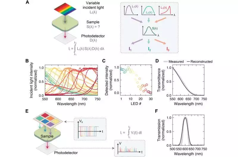
spectral measurement using arrays with a lot of colors A) Schematic portraying the idea driving conveyance estimation utilizing variable occurrence illumination and a solitary photodetector (B) EL device spectra (table S3) and photodetector readings that were used to reconstruct the sample transmittance (D) E) Schematic illustrating the idea behind time-multiplexed transmittance measurement made possible by applying a series of phase-shifted gate voltage waveforms to each device in a 2 x 3 EL array F) A spectral transmittance reconstruction based on the idea in (E) . Credit: Science Advances (2023). DOI: 10.1126/sciadv.adg1607
Reconstructive spectral measurement and imaging The team used active spectral measurements to demonstrate the scalability and adaptability of the device platform as well as the variety of electroluminescence spectra that could be obtained. By passing broadband light through an unknown sample, for instance, they measured the transmission spectrum. In another instance, they measured the spectral data using reconstructive spectrometry to algorithmically recover the spectral data. The special and intrinsically beat nature of the instrument permitted them to direct substitute ghostly estimations and accomplish quick otherworldly estimations without exchanging gadgets.
Wang et al. carried out reconstructive spectral measurements after utilizing the apparatus for spectral imaging. A silicon charge-coupled camera took pictures of the samples while the electroluminescence arrays provided the light. Because they are possible for a variety of adaptive sensing applications, they also managed to achieve spectral imaging of semi-transparent biological samples and maintain the scale of miniaturized light-emitting arrays at the nanoscale and microscale on a chip.
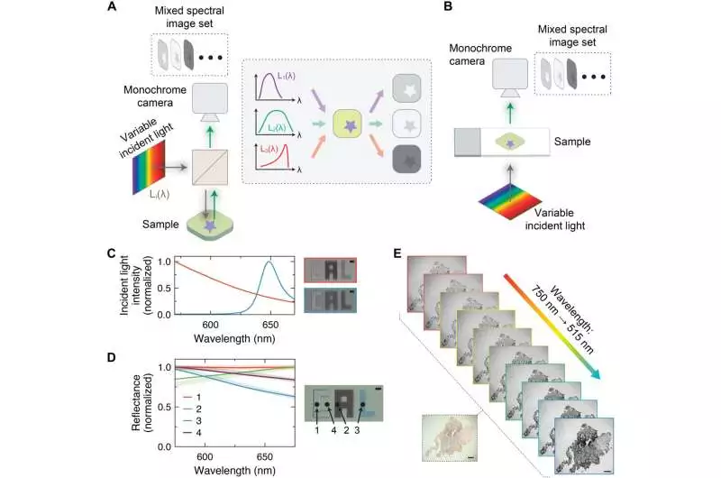
Phantom imaging with profoundly colorful exhibits Microscale (A) reflected-light and (B) transmitted-light spectral imaging with variable incident illumination and a monochrome camera are depicted schematically. C) An illustration of various reflected-light microscope images and incident light spectra 40 m scale bar (D): Utilizing the emitters in Table S4, reconstructed reflectance spectra at various locations on the sample depicted in the optical micrograph. 40-m scale bar (E): A transmitted-light imaging setup’s spectral data cube for a sample of human tissue Scale bars, 100 m. Credit: Science Advances (2023). DOI: 10.1126/sciadv.adg1607
Vivian Wang and her colleagues created this straightforward and scalable instrument for housing light-emitting device arrays with highly multiplexed emission across the visible and infrared wavelengths. The scientists integrated the multicolor devices completely with pulsed-driven metal-oxide semiconductor capacitors.
In order to investigate spectral reflectance and transmission imaging as well as the spectral properties of samples, this platform serves as a random source of variable light emission. The researchers further developed otherworldly imaging precision and inclusion with frightfully tuned materials, for example, colloidal quantum dabs and perovskite nanomaterials, or slender brilliant movies created by combinatorial testimony.
In addition to the visible spectrum, this work has the potential to be extended to more extreme wavelengths. The pixels in the light discharging exhibits can be separately tended to, permitting materials researchers to utilize the instruments and produce light with adjustable examples in recurrence and existence for multi-faceted phantom estimations.
More information: Vivian Wang et al, Highly multicolored light-emitting arrays for compressive spectroscopy, Science Advances (2023). DOI: 10.1126/sciadv.adg1607
Chuan Wang et al, User-interactive electronic skin for instantaneous pressure visualization, Nature Materials (2013). DOI: 10.1038/nmat3711


