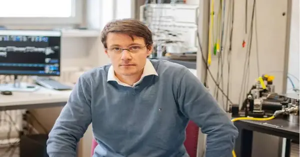
At the point when Mickael Perrin began his logical profession a long time ago, he had absolutely no chance of realizing he was directing exploration in a space that would draw wide open interest a couple of years after the fact: quantum hardware. “At that point, physicists were simply beginning to discuss the capability of quantum advancements and quantum PCs,” he reviews.
“Today there are many new businesses around here, and legislatures and organizations are putting billions into fostering innovation further. We are currently seeing the main applications in software engineering, cryptography, correspondence, and sensors.” Perrin’s exploration is opening up one more field of utilization: power creation utilizing quantum impacts with right around zero energy misfortune. To accomplish this, the 36-year-old researcher joins two generally separate disciplines of material science: thermodynamics and quantum mechanics.
In the previous year, the nature of Perrin’s examination and its true capacity for future applications brought him two honors. He got not just one of the ERC Beginning Awards that are so exceptionally pursued by youthful specialists, but in addition an Eccellenza Scholarly Cooperation of the Swiss Public Science Establishment (SNS). He presently drives an examination gathering of nine at Empa, similar to an Associate Teacher of Quantum Gadgets at ETH Zurich.
“Generally speaking, the larger and more costly the machine you’ll need to build the structure, the smaller the structure you wish to build, Because something almost always goes wrong, nanofabrication and experimental physics require a great deal of imagination and perseverance.”
Explains Perrin. Lithography machines, for example, which are used to pattern complex mini-circuits on microchips.
Multiple times less than a hair
Perrin lets us know that he never viewed himself as having a characteristic gift for science. “It was mostly interest that pushed me toward physical science. I needed to acquire a superior comprehension of how our general surroundings function, and physical science offers fantastic devices for doing exactly that.” Subsequent to completing secondary school in Amsterdam, he started a degree in applied physical science at Delft College of Innovation (TU Delft) in 2005. Right all along, Perrin was more keen on substantial applications than hypotheses.
It was while concentrating under Herre van der Zant, a trailblazer in the field of quantum hardware, that Perrin originally encountered an interest in designing small gadgets at the microscale and nanoscale. He before long perceived the vast potential outcomes introduced by atomic hardware, since circuits have totally various attributes based on the particles and materials chosen and can be utilized as semiconductors, diodes, or sensors.
While reading up for his doctorate, Perrin invested a lot of energy in the nanolab cleanroom at TU Delft—constantly wrapped in a white full-body in general—to forestall the smaller than normal gadgets from being tainted by hairs or residue particles. The cleanroom gave the mechanical foundation to construct machines a couple of nanometers in size (multiple times less than the width of a human hair).
“When in doubt, the more modest the design you need to construct, the greater and more costly the machine you should do as such,” makes sense of Perrin. Lithography machines, for instance, are utilized to design complex small-scale circuits on computer chips. “Nanofabrication and test material science require a great deal of innovativeness and tolerance, since something almost consistently turns out badly,” says Perrin. “However, the weird and startling outcomes frequently end up being the most invigorating.”
Graphene: A wonder material
A year after finishing his doctorate, Perrin got a post at Empa in the research facility of Michel Calame, a specialist in coordinating quantum materials into nanogadgets. From that point forward, Perrin—a French and Swiss public figure—has lived in Dübendorf with his accomplice and two girls. “Switzerland was a decent decision for me because of multiple factors,” he says. “The exploration framework is unmatched.”
Empa, ETH Zurich, and the IBM Exploration Center in Rüschlikon give him all that he really wants to create nanostructures, as well as the estimating instruments to test them. “Likewise, I’m an outside sort. I love the mountains and frequently go strolling and skiing with my family.” Perrin is a sharp stone climber as well. In some cases, he takes himself off, moving in distant valleys for a really long time at a time, often in France, which is his family’s nation of origin.
At Empa, this youthful analyst had the opportunity to keep exploring different avenues regarding nanomaterials. A specific material before long was pulled into his specific consideration: graphene nanoribbons, a material produced using carbon molecules that is pretty much as slim as the singular particles. These nanoribbons were fabricated with the best accuracy by Roman Fasel’s gathering at Empa. Perrin had the option to show that these strips have interesting properties and can be utilized for an entire pontoon of quantum innovations.
Simultaneously, he started to take an interest in changing heat into electrical energy. In 2018, it was demonstrated as a matter of fact that quantum impacts can be utilized to effectively change nuclear power. Up to now, the issue has been that these advantageous actual properties show up just at extremely low temperatures—nearly outright zero (0 Kelvin; -237 °C). This is of little relevance to potential future applications, for example, in cell phones or minisensors.
Perrin was dodging this issue by utilizing graphene nanoribbons. Their particular actual properties imply that temperature smallerly affects the quantum impacts—and subsequently the ideal thermoelectric impacts—than is the situation with different materials. His gathering at Empa was soon ready to show that the quantum impacts of graphene nanoribbons are generally safeguarded even at 250 Kelvin, for example, 23°C. Later on, the framework is supposed to work at room temperature as well.
Lower power utilization because of nanotubes
There are still many difficulties to beat before the innovation will empower our cell phones to utilize less power. Outrageous scaling down implies that extraordinary parts continue to be expected to guarantee that the constructed frameworks really work. Perrin, along with associates from China, the U.K., and Switzerland, has as of late demonstrated the way that carbon nanotubes only one nanometer in width can be coordinated into those frameworks as anodes.
Nonetheless, Perrin estimates that it will require essentially an additional 15 years before these sensitive and profoundly convoluted materials can be produced at scale and consolidated into gadgets. “My point is to figure out the essential reason for applying this innovation. Really, at that time, can we check its true capacity for reasonable purposes?”
Provided by Swiss National Science Foundation


