Analysts at the University of Toronto and the Barcelona Institute of Science and Technology have as of late made new arrangements for handling perovskite photodetectors that show amazing efficiencies and reaction times. These photodetectors, presented in a paper distributed in Nature Electronics, have a novel structure that forestalls the development of deformities between their various layers.
“There is developing interest in 3D territory imaging for independent driving and consumer gadgets,” Edward H. Chief told TechXplore. “We have filled in collectively for quite a long time on finding new materials that empower light detecting advances, for example, cutting edge picture sensors, and endeavoring to steer these toward a path that could have a business and cultural effect.”
“When photogenerated electrons and holes are absorbed by the perovskite active layer, they are removed through electron and hole transport layers. These charge carriers must flow quickly across the devices, including the transport layers, in order to achieve fast reaction times. Because of its high crystallinity and mobility, nickel oxide (NiOx) is an excellent choice for hole transport layer (HTL).”
Maral Vafaie
Photodetectors, detecting gadgets that identify or respond to light, can have various profoundly important applications. They can be integrated into automated frameworks, autonomous vehicles, buyer gadgets, natural detecting innovation, fiber optic correspondence frameworks, and security frameworks, for example.
“In these applications, quick photodetection is expected in frequency ranges past human vision,” Amin Morteza Najarian said. “The circuitous bandgap, a property of silicon’s band structure that produces frail retention (thus a requirement for thick silicon) in the close to infrared, is a property of silicon’s band structure that produces frail retention (thus a requirement for thick silicon) in the close to infrared.”

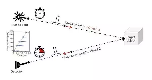
Working Rule of Light Detection and Ranging: LiDAR calculates the time it takes light to travel to an object and then disperse back into the finder. The speed of light is utilized to make an interpretation of worldly data into spatial data.
In a progression of starting computational examinations, Sargent and his group recognized a paired perovskite with high transporter versatility and a high retention coefficient that could rival presently utilized materials regarding both proficiency and speed. The photodetector presented in their new paper depends on this recently recognized, dynamic material.
“At the point when light is consumed by the perovskite dynamic layer, the photogenerated electrons and openings are removed through electron and opening vehicle layers,” said coauthor Maral Vafaie. To accomplish quick reaction times, these charge transporters should move quickly across the gadgets, including the vehicle layers. “Nickel oxide (NiOx) is characterized by high crystallinity and versatility, making it an ideal choice for opening vehicle layer (HTL).”
At the point when they initially began testing their gadgets, the scientists observed that there was a compound incongruence between the laid out enemy of oxidation system for PbSn perovskites and the NiOx layer. They hence concocted a strategy to eliminate oxygen from the gadget, changing over undesirable tin species and abandoning it to guarantee no unsafe buildup.
In their starting assessments, the photodetectors made by Sargent, Najarian, Vafaie, and their partners accomplished extremely encouraging outcomes, both as far as quantum efficiencies and reaction times. The group likewise demonstrated the way that their gadgets can determine sub-millimeter distances with a normal 50 m standard deviation.
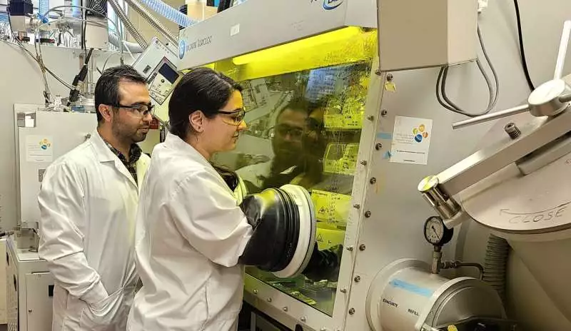
PbSn perovskites for LiDAR are created by a U of T undergrad and postdoc (Maral and Amin).Najarian and colleagues
“We showed that photodetectors created utilizing paired perovskites convert close to infrared light into electrical signals with a proficiency better than 85% with a reaction time quicker than a small part of a nanosecond,” Sargent and Morteza Najarian said. “This is a 100-fold improvement compared with the recently detailed arrangement of photodetectors. We feature these exhibition measurements in spatially settling sub-millimeter distances, i.e., giving profundity goal. “
Later on, the new arrangement handling perovskite photodetectors made by Sargent, Morteza Najarian, and their partners could be important for making LiDAR innovation (i.e., devices for deciding variable distances among items) and sensors for independent vehicles or robots. In the interim, the analysts intend to keep looking for favorable materials and planning new parts for detecting advances.
“In lengthy reach light location and going (LiDAR) applications, just a little part of the dispersed light from the items comes to the photodetector,” Sargent and Morteza Najarian added. “In the event that one moves brightening and detecting to the short-wave infrared locale (e.g., 1550 nm), a higher force of enlightening light becomes conceivable without presenting eye security issues. We are chipping away at the cutting edge III-V semiconductors considering this.”
More information: Amin Morteza Najarian et al, Sub-millimetre light detection and ranging using perovskites, Nature Electronics (2022). DOI: 10.1038/s41928-022-00799-7
Journal information: Nature Electronics


