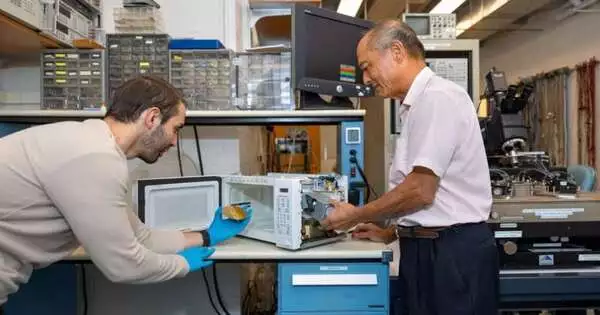
A family microwave designed by a Cornell design teacher is assisting with concocting the up and coming age of cellphones, PCs, and other hardware after the development was demonstrated to beat a significant test conducted by the semiconductor business.
The examination is nitty-gritty in a paper distributed in Applied Material Science Letters. The lead creator is James Hwang, an exploration teacher in the branch of materials science and design.
As microprocessors keep on contracting, silicon should be doped, or blended, with higher concentrations of phosphorus to create the ideal current. Semiconductor makers are currently moving toward a fundamental cutoff wherein conventional methods of warming extremely doped materials no longer produce reliably utilitarian semiconductors.
“A few companies are now manufacturing 3 nanometer semiconductor materials. Leading manufacturers like as TSMC and Samsung may be able to scale down to 2 nanometers using this new microwave method.”
James Hwang, a research professor in the department of materials science and engineering.
The Taiwan Semiconductor Assembling Organization (TSMC) hypothesized that microwaves could be utilized to enact the overabundance of dopants, yet very much like with home microwaves that occasionally heat food unevenly, past microwave annealers created “standing waves” that forestalled steady dopant initiation.
TSMC joined forces with Hwang, who changed the microwave to specifically control where the standing waves happen. Such accuracy takes into consideration the legitimate initiation of the dopants without unreasonable warming or harm of the silicon precious stone.
This revelation could be utilized to create semiconductor materials and hardware showing up around the year 2025, said Hwang, who has documented two licenses for the model.
“A couple of makers are right now creating semiconductor materials that are 3 nanometers,” Hwang said. “This new microwave approach might possibly empower driving makers, for example, TSMC and Samsung, to downsize to only 2 nanometers.”
The advancement could change the calculation of semiconductors utilized in microprocessors. For over 20 years, semiconductors have been made to stand up like dorsal blades so that more can be pressed on every CPU, but producers have as of late tried different things with another design in which semiconductors are stacked on a level plane. The unreasonably doped materials empowered by microwave tempering would be vital to the new design.
More information: Chun-Hsiung Tsai et al, Efficient and stable activation by microwave annealing of nanosheet silicon doped with phosphorus above its solubility limit, Applied Physics Letters (2022). DOI: 10.1063/5.0099083
Journal information: Applied Physics Letters


