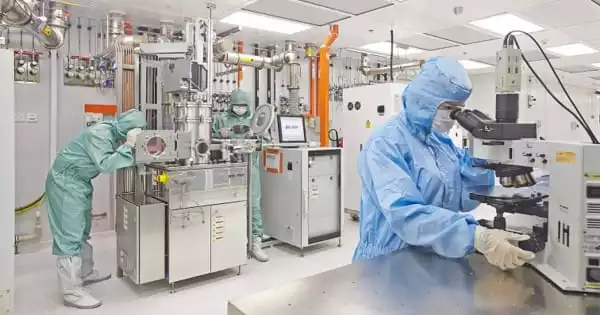
A team of researchers from The University of Manchester’s National Graphene Institute (NGI) and the National Physical Laboratory (NPL) established room-temperature ferroelectricity in slightly twisted 2D transition metal dichalcogenides (TMDs).
This property, in conjunction with TMDs’ exceptional optical capabilities, can be exploited to create multi-functional optoelectronic devices like as transistors and LEDs with built-in memory functionalities on the nanometre length scale.
Ferroelectrics are materials that have two or more electrically polarisable states that can be switched reversibly by applying an external electric field. This material feature makes it perfect for non-volatile memory, microwave devices, sensors, and transistors. Until recently, only films thicker than 3 nanometres could accomplish out-of-plane switchable ferroelectricity at ambient temperature.
It’s incredibly thrilling to show that this basic twisting tool may design novel features in 2D crystals. With such a large selection of 2D crystals to pick from, we have nearly limitless possibilities for creating properly suited artificial materials.
Astrid Weston
2D heterostructures
Since the isolation of graphene in 2004, academics have investigated a wide number of new 2D materials with a wide range of intriguing features. These atomically thin 2D crystals can be piled on top of one another to form heterostructures, or artificial materials with specific functionality.
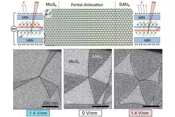
Recently, a team of NGI researchers, in conjunction with NPL, revealed that below a twist angle of 2o, atomic lattices physically reassemble to form sections (or domains) of precisely stacked bilayers separated by boundaries of locally generated strain. A tessellated pattern of mirror-reflected triangular domains is formed when two monolayers are placed parallel to each other. Most crucially, the two neighboring domains have asymmetric crystal symmetry, resulting in asymmetry in their electrical characteristics.
Ferroelectric switching at room temperature
The scientists demonstrated that the domain structure formed by low-angle twisting hosts interfacial ferroelectricity in bilayer TMDs in their paper, which was published in Nature Nanotechnology. Kelvin probe force microscopy indicated that neighboring domains are polarized in different directions, and electrical transport experiments demonstrated consistent ferroelectric switching at ambient temperature.
The researchers went on to develop a scanning electron microscope (SEM) approach with improved contrast by utilizing backscattered electron signal. This allowed for the application of an electric field in-situ while imaging changes to the domain structure in a non-invasive manner, providing critical information on how the domain flipping process operates. The boundaries between oppositely polarised domains were discovered to expand and contract depending on the sign of the applied electric field, resulting in a considerable redistribution of the polarised states.
This work clearly shows how the twist degree of freedom can be used to create atomically thin optoelectronics with customized and multi-functional features.
Two-dimensional transition-metal dichalcogenide (TMDC) materials provide a novel option for university laboratories to quickly access semiconductor devices such as field-effect transistors, diodes, and sensors. Final semiconductor devices can be created using photo- or e-beam lithography techniques, which are widely used in the lab, ranging from mechanically exfoliated flakes to CVD-grown monolayer films. A new concept for next-generation information processing hardware elements with low-power and quick operation transistor/memory devices is being tested.
Wide scope for tailored 2D materials
Astrid Weston, the lead author, stated: “It’s incredibly thrilling to show that this basic twisting tool may design novel features in 2D crystals. With such a large selection of 2D crystals to pick from, we have nearly limitless possibilities for creating properly suited artificial materials.”
Dr. Eli G Castanon, a co-author, added: “It was quite thrilling to be able to study the arrangement and behavior of ferroelectric domains in materials with nanometre thickness using KPFM and SEM. The progress of characterization techniques, together with the numerous possibilities for the formation of innovative heterostructures of 2D materials, provides the path for many industries to reach new capabilities at the nanoscale.”
The electronics industry, particularly the semiconductor business, is constantly on the lookout for smaller and more efficient components. Because of their widespread use in the photovoltaic and computer industries—from transistors to solar cells—there is a growing interest in discovering new semiconductor materials and incorporating them into existing technologies.
There are numerous acceptable semiconductor materials, each with subtle differences in their characteristics that bring benefits and drawbacks in their specific applications. Because industry entrepreneurs want to improve semiconductor efficiency, there is a growing interest in inventing new semiconducting materials.


