Scientists have fostered another all-optical strategy for driving variously thick nanolaser clusters. The methodology could enable chip-based optical correspondence to connect that cycle and move data faster than current electronic-based devices.
“The advancement of optical interconnects furnished with high-thickness nanolasers would further develop data handling in the server farms that get data across the web,” said research group pioneer Myung-Ki Kim from Korea College.
“This could enable the streaming of high-quality films, enable a wider range of intuitive web-based experiences and games, accelerate the expansion of the Web of Things, and provide the quick network required for massive data examination.”
“The creation of optical interconnects outfitted with high-density nanolasers might boost information processing in data centers that move data across the internet,”
Team leader Myung-Ki Kim from Korea University.
The examination, distributed in Optica, shows that thickly coordinated nanolaser exhibits—iin which the lasers are only 18 microns apart—ccan be completely determined and modified with light from a solitary optical fiber.
“Optical gadgets coordinated onto a chip are a promising option in contrast to electronic coordinated gadgets, which are battling to stay aware of the present information handling requests,” said Kim.
“By killing the huge and complex anodes normally used to drive laser clusters, we decreased the general components of the laser exhibit while likewise taking out the intensity age and handling delays that accompany cathode-based drivers.”
Supplanting anodes with light
The new nanolasers could be utilized in optically coordinated circuit frameworks that identify, create, send, and handle data on a CPU through light. Rather than the fine copper wires utilized in electronic chips, optical circuits utilize optical waveguides, which permit much higher transfer speeds while creating less intensity. Nonetheless, because the size of optically coordinated circuits is rapidly approaching the nanometer system, better approaches to driving and controlling their nano-sized light sources are required.
To produce light, lasers should be provided with energy in a cycle called siphoning. For nanolaser clusters, this is commonly achieved by involving a couple of cathodes for every laser inside an exhibit, which requires huge on-chip space and energy utilization while likewise causing handling delays.
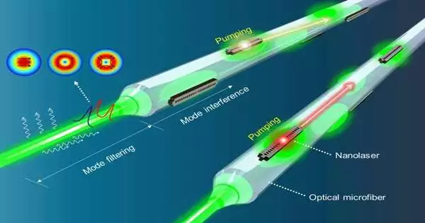
To beat this basic limit, the scientists supplanted these cathodes with a novel optical driver that makes programmable examples of light through impedance. This siphon light goes through an optical fiber, onto which nanolasers are printed.
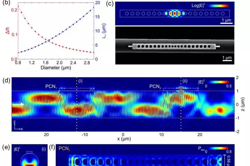
These recreation pictures show how the light impedance design connects with the nanolaser exhibits. (a) A schematic of spatial impedance somewhere in the range of TE00 and TE01 modes along the microfiber Here, two photonic gem nanobeam lasers (PCN1 and PCN2) are joined to the outer layer of the microfiber in a line. (b) Difference in viable refractive files (n) of TE00 and TE01 modes and corresponding half beat length (L);(c) SEM image of a manufactured InGaAsP PCN laser and log |E|2 profile of PCN pit mode in the xy-plane.(d, e) 2 profiles of the siphon bar in the x- and y-planes, separately, where the bar spreads from left to right (f) Retained power thickness profiles along the xy-plane at the upward focus of PCNs Credit: Korea College
To demonstrate this methodology, the scientists utilized a high-goal moving printing strategy to create various photonic gem nanolasers separated by 18 microns. These exhibits were applied to the outer layer of a 2-micron-wide optical microfiber.
This must be finished in a manner that exactly aligns the nanolaser clusters with the impedance design. The impedance example could likewise be changed by changing the driving bar’s polarization and heartbeat width.
Laser driving with a solitary fiber
The tests revealed that the plan allowed multiple nanolaser clusters to be driven by light passing through a single fiber.The results agreed with mathematical predictions and demonstrated that the printed nanolaser exhibits could be completely constrained by siphon bar impedance designs.
“Our all-optical laser driving and programming innovation can likewise be applied to chip-based silicon photonics frameworks, which could assume a vital part in the improvement of chip-to-chip or on-chip optical interconnects,” said Kim.
“In any case, it would be important to demonstrate how freely the methods of a silicon waveguide can be controlled.” In the event that this should be possible, it would be an immense leap forward in the development of on-chip optical interconnects and optically coordinated circuits.
More information: Myung-Ki Kim et al, Three-dimensional programming of nanolaser arrays through a single optical microfiber, Optica (2022). DOI: 10.1364/OPTICA.471715
Journal information: Optica


