Specialists at the Georgia Organization of Innovation have fostered a light-based method for printing nano-sized metal designs that is fundamentally quicker and less expensive than any innovation presently accessible. A versatile arrangement could change a logical field long dependent on innovations that are restrictively costly and slow. The advancement can possibly free new innovations once again from labs and into the world.
Mechanical advances in many fields depend on the capacity to print metallic designs that are nano-sized—a scale many times less than the width of a human hair. Sourabh Saha, aide teacher in the George W. Woodruff School of Mechanical Designing, and Jungho Choi, a Ph.D. understudy in Saha’s lab, fostered a strategy for printing metal nanostructures that is multiple times quicker and multiple times less expensive than the ongoing ordinary technique.
Their exploration is distributed in the Progressed Materials diary.
Printing metal on the nanoscale—a method known as nanopatterning—takes into consideration the production of special designs with fascinating capabilities. It is pivotal for the advancement of numerous innovations, including electronic gadgets, sunlight-based energy transformation, sensors, and different frameworks.
A video of nanoprinting with superluminescent light projection (SLP). Credit: Georgia Institute of Technology
It is, for the most part, accepted that extreme-focus light sources are expected for nanoscale printing. Yet, this sort of hardware, known as a femtosecond laser, can cost up to a portion of 1,000,000 bucks and is excessively costly for most exploration labs and independent ventures.
“As an academic local area, we don’t make enough of these nanomaterials rapidly and moderately, and for that reason, promising innovations frequently stay restricted to the lab and don’t get converted into certifiable applications,” Saha said.
“The inquiry we needed to respond to is, ‘Do we truly need a focused energy femtosecond laser to print on the nanoscale?’ Our speculation was that we needn’t bother with that light source to get the sort of printing we need.”
They looked for a minimal-cost, low-power light that could be engaged in a manner like femtosecond lasers and picked superluminescent light-discharging diodes (SLEDs) for their business accessibility. SLEDs discharge light that is a billion times less extraordinary than that of femtosecond lasers.
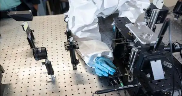
Saha and Choi set off on a mission to make a unique projection-style printing innovation, planning a framework that changes over-computerized pictures into optical pictures and shows them on a glass surface. The framework works like computerized projectors, however, creating pictures that are all the more pointedly engaged. They utilized the interesting properties of the superluminescent light to create strongly engaged pictures with negligible imperfections.
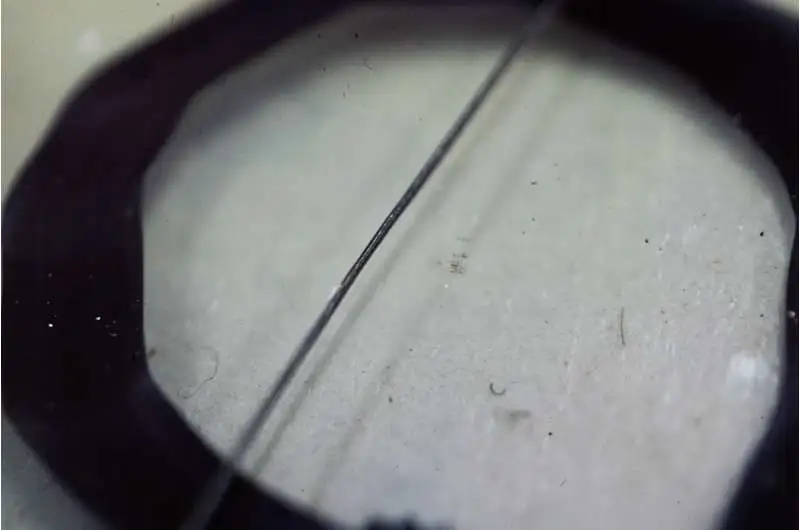
Size examination between human hair (~100 micrometer thickness) versus printed silver cushion on a glass coverslip. Credit: Georgia Institute of Technology
They then fostered a reasonable ink arrangement comprised of metal salt and added different synthetics to ensure the fluid could ingest light. At the point when light from their projection framework hit the arrangement, it caused a substance response that changed the salt arrangement into metal. The metal nanoparticles adhere to the outer layer of the glass, and the agglomeration of the metal particles makes the nanostructures. Since it is a projection kind of printing, it can print a whole construction in one go, as opposed to point by point, making it a lot quicker.
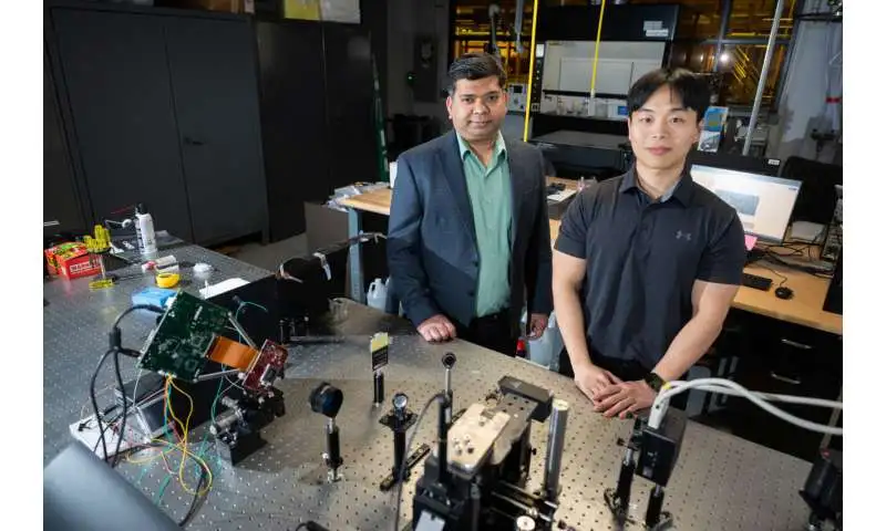
Assistant professor Sourabh Saha and Jungho Choi (Ph.D. student) in front of their superluminescent light projection system at Georgia Tech. Credit: Georgia Institute of Technology
Subsequent to testing the strategy, they found that projection-style nanoscale printing is conceivable even with low-power light, however, provided that the pictures are strongly engaged. Saha and Choi accept that analysts can promptly repeat their work utilizing economically accessible equipment. Not at all like an expensive femtosecond laser, the kind of SLED that Saha and Choi utilized in their printer costs about $3,000.
“As of now, just top colleges approach these costly advancements, and, surprisingly, at that point, they are situated in shared offices and are not generally accessible,” Choi said. “We need to democratize the capacity of nanoscale 3D printing, and we trust our examination opens the entryway for more prominent admittance to this sort of interaction for a minimal price.”
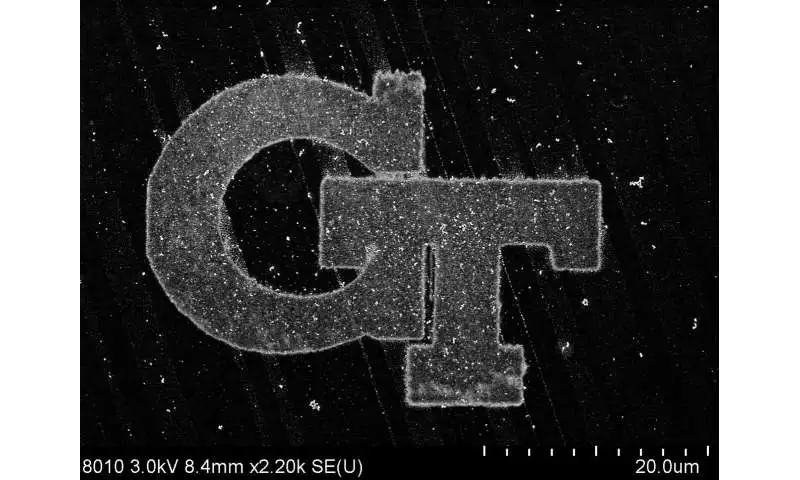
Scanning electron microscope image of printed silver GT pattern. Credit: Georgia Institute of Technology
The scientists say their strategy will be especially helpful for individuals working in the fields of gadgets, optics, and plasmonics, which all require an assortment of perplexing metallic nanostructures.
“I think the measurements of cost and speed have been significantly underestimated by mainstream researchers who chip away at the creation and assembly of minuscule designs,” Saha said.
“In reality, these measurements are significant with regards to deciphering disclosures from the lab to industry. Just when we have production strategies that consider these measurements, can we completely influence nanotechnology for cultural advantage?”
More information: Jungho Choi et al, Scalable Printing of Metal Nanostructures through Superluminescent Light Projection, Advanced Materials (2023). DOI: 10.1002/adma.202308112


