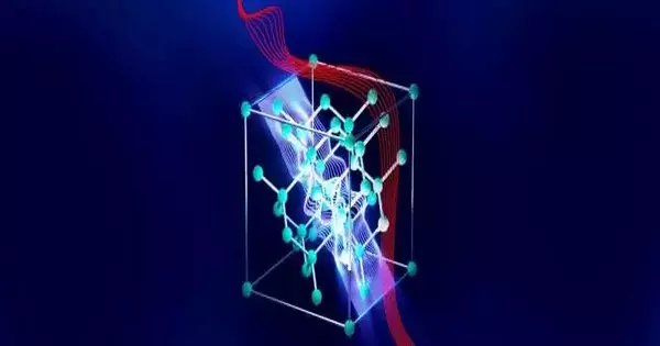
Analysts at Purdue University have found new waves with picometer-scale spatial varieties of electromagnetic fields that can spread in semiconductors like silicon. The exploration group, led by Dr. Zubin Jacob, Elmore Academic Partner of Electrical and PC Design, and Branch of Physical Science and Cosmology, distributed their discoveries in an Actual Survey. applied in a paper named “Picophotonics: Odd Atomistic Waves in Silicon.”
“The term tiny derives from the length of a micron, which is many times less than a meter.”Our work is for light-matter connection inside the picoscopic system, which is far more modest, where the discrete plan of nuclear grids changes light’s properties in amazing ways,” says Jacob.
These charming discoveries show that normal media have an assortment of rich light-matter connection peculiarities at the atomic level. The utilization of picophotonic waves in semiconducting materials might lead analysts to plan new, useful optical gadgets, considering applications in quantum advances.
“This represents a significant departure from the classical treatment of light flow used in nanophotonic; the quantum nature of light’s behavior in materials is critical for the emergence of Pico photonics phenomena.”
Dr. Zubin Jacob, Elmore Associate Professor of Electrical and Computer Engineering
Light-matter connection in materials is key to a few photonic gadgets, from lasers to finders. Throughout the last 10 years, nanophotonics—the investigation of how light streams on the nanometer scale in designed designs, for example, photonic gems and metamaterials—has prompted significant advances. This current investigation may be caught within the domain of the old-style nuclear matter hypothesis.The ongoing finding prompting picophotonics was made conceivable by a significant leap forward involving a quantum hypothesis of atomistic reaction in issue. The group comprises Jacob as well as Dr. Sathwik Bharadwaj, a research researcher at Purdue College, and Dr. Todd Van Mechelen, a previous postdoc at Purdue College.
The field’s long-standing puzzle was the missing link between nuclear grids, their balances, and the role it plays on profoundly picoscopic light fields.To solve this mystery, the hypothesis group developed a Maxwell Hamiltonian system of issue in conjunction with a quantum hypothesis of light-induced reaction in materials.
“This is a vital shift from the old style treatment of light streams applied in nanophotonics,” says Jacob. “The quantum idea of light’s conduct in materials is the key to the rise of picophotonic peculiarities.”
Bharadwaj and colleagues demonstrated that, hidden among the usual notable electromagnetic waves, new strange waves emerge in the nuclear grid.These light waves are profoundly oscillatory, even inside one key structure block of the silicon gem (sub-nanometer length scale).
“Normal materials themselves have rich inborn gem grid balances, and light is firmly affected by these balances,” says Bharadwaj. “The immediate next goal is to apply our hypothesis to a wide range of quantum and topological materials and tentatively test the presence of these new waves.”
“Our gathering has been driving the boondocks of exploration on pico-scale electrodynamic fields inside issues at the atomic level,” says Jacob. “We have as of late started the picoelectrodynamic hypothesis organization, where we are uniting different analysts to investigate perceptible peculiarities coming from tiny pico-electrodynamic fields inside an issue.”
More information: Sathwik Bharadwaj et al, Picophotonics: Anomalous Atomistic Waves in Silicon, Physical Review Applied (2022). DOI: 10.1103/PhysRevApplied.18.044065


