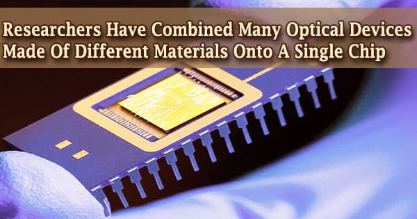
Researchers have devised a method for assembling several micron-scale optical devices very close together on a single chip that is incredibly precise. The novel method might one day allow for high-volume production of chip-based optical systems, allowing for smaller optical communications devices and improved imagers.
“The development of electronics that are based on silicon transistors has enabled increasingly more powerful and flexible systems on a chip,” Dimitars Jevtics from the University of Strathclyde in the UK. “Optical systems on a chip, on the other hand, need the integration of many materials on a single chip and, as a result, have not experienced the same scale of development as silicon electronics.”
The development of electronics that are based on silicon transistors has enabled increasingly more powerful and flexible systems on a chip.
Dimitars Jevtics
Jevtics and colleagues explain their innovative transfer printing technology in the Optica Publishing Group journal Optical Materials Express, demonstrating its capacity to install devices comprised of several materials on a single chip, all within a footprint identical to the devices themselves. Unlike existing techniques, which are usually confined to a single material, this new method gives a toolbox of materials from which future system designers may choose.
“On-chip optical communications, for example, will require the assembly of optical sources, channels, and detectors onto sub-assemblies that can be integrated with silicon chips,” said Jevtics.
“Our transfer printing process could be scaled up to integrate thousands of devices made from different materials onto a single wafer. Micron-scale optical devices might be integrated into future computer chips for high-density communications or lab-on-a-chip bio-sensing platforms as a result of this.”
A better way to pick and place
One of the most difficult aspects of putting several devices on a chip is trying to fit them in close proximity without interfering with other devices on the chip. To do so, the researchers devised a reversible adhesion approach in which a device is picked up and removed from its growing substrate before being deposited on a new surface.
The novel technology picks up an optical device from its substrate using a soft polymer stamp set on a robotic motion control stage. The substrate, which will be deposited on top of it, is then positioned under the suspended device and precisely aligned with the help of a microscope.
The two surfaces are brought into contact after they are suitably aligned, releasing the device from the polymer stamp and depositing it on the target surface. This strategy was made possible by advancements in precise micro-assembly robots, nano fabrication techniques, and microscope image processing.
“By carefully designing the geometry of the stamp to match the device and controlling the stickiness of the polymer material, we can engineer whether a device will be picked up or released,” said Jevtics. “When optimized, this method causes minimal harm and may be scaled up utilizing automation to meet wafer-scale manufacturing requirements.”
Creating a densely packed chip
The researchers demonstrated the novel approach by combining optical resonators made of aluminum gallium arsenide, diamond, and gallium nitride on a single chip. The optical transmission of these optical resonators was excellent, indicating that the integration was successful.
They also employed the printing method to make semiconductor nanowire lasers by arranging nanowires in spatially dense patterns on host surfaces. The spatial precision of the spacing between the nanowires was measured using scanning electronic microscopy, and it was found to be in the 100-nanometer range. They were able to develop a multi-wavelength nanolaser system by putting semiconductor nanowires on silicon dioxide.
“As a manufacturing technique, this printing approach is not limited to optical devices,” said Jevtics. “We hope that electronics specialists will also see possibilities for how it could be applied in future systems.”
The researchers are now aiming to duplicate these findings with a bigger number of devices in order to demonstrate that it works at a broader scale. They also intend to integrate their transfer printing method with an automated alignment process they previously created to allow for the quick measurement, selection, and transfer of hundreds of isolated devices for imaging and hybrid optical circuits applications.
This work was funded by the Engineering and Physical Sciences Research Council (EP/R03480X/1, EP/P013597/1, EP/P013570/1); European Commission (Grant No. 828841 ChipAI-H2020-FETOPEN-2018-2020, Grant No. 829116 SuperPixels -H2020-FETOPEN-2018-2020) and the Royal Academy of Engineering under the Research Chairs and Senior Research Fellowships scheme. Jack Smith’s PhD studentship is co-funded by Fraunhofer UK.


