For around 20 years, it has been feasible to change surfaces through nanoparticles with the goal that they concentrate or control light in an ideal manner or trigger different responses. Such optically dynamic nanostructures can be tracked down in sun-based cells and natural or substance sensors, for instance.
To extend the scope of uses for these nanostructures, specialists at the Foundation of Electron Microscopy and Nanoanalysis (Graz College of Innovation) and the Graz Focus of Electron Microscopy (ZFE) have been working for over 10 years on assembling level nanostructures, yet specifically mind-boggling, detached 3D designs.
The group led by Harald Board, Verena Reisecker, and David Kuhness has accomplished two leaps forward. It is currently conceivable to definitively reproduce the expected shapes and sizes of nanostructures ahead of time to accomplish desired optical properties, which can then be precisely delivered. The group has additionally figured out how to totally eliminate substance pollution integrated during introductory creation without adversely influencing the 3D nanoarchitectures.
The discoveries are distributed in the journal Progressed Practical Materials.
“The major issue in recent years has been transferring 3D structures into high-purity materials without compromising the morphology. The 3D component of this development leap allows for new optical effects and application concepts. Nanoprobes or optical tweezers with nanometer-scale precision are now available.”
Harald Plank
The experimentation technique becomes pointless.
Up to this point, 3D nanostructures called for a tedious experimentation process until the item uncovered the ideal optical properties. This trouble has at last been dispensed with. “The consistency among reenactments and genuine plasmonic resonances of an extensive variety of nanoarchitectures is extremely high,” makes sense of Board. “This is an immense forward-moving step. The difficult work of the most recent couple of years has at long last paid off.”
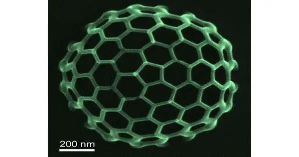
The innovation is presently the only one on the planet that can be utilized to create complex 3-layered structures with individual highlights less than 10 nanometers in a controlled, single-step strategy on practically any surface. For correlation, the littlest infections are around 20 nanometers in size.
“The greatest test as of late was to move the 3D structures into high-virtue materials without obliterating the morphology,” makes sense of Board. “This advancement jump empowers new optical impacts and application ideas because of the 3D angle.” Nanoprobes or optical tweezers with sizes in the nanometer range are presently reachable.
Exactly controlled electron pillar
The scientists utilize a centered electron pillar-initiated affidavit to deliver the nanostructures. The important surface is exposed to extraordinary gases under vacuum conditions. A finely engaged electron shaft divides the gas particles, whereupon parts of them change into a strong state and stick to the ideal area.
“By definitively controlling bar developments and openness times, we can deliver complex nanostructures with cross-section or sheet-like structure blocks in a single step,” makes sense of Board. By stacking these nano-volumes on top of one another, three-layered designs can eventually be built.
More information: Verena Reisecker et al, Spectral Tuning of Plasmonic Activity in 3D Nanostructures via High‐Precision Nano‐Printing, Advanced Functional Materials (2023). DOI: 10.1002/adfm.202310110


