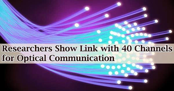
A silicon-based optical communication link that combines two multiplexing technologies to create 40 optical data channels that may transfer data simultaneously has been demonstrated by researchers.
The new chip-scale optical link can move the equivalent of 100,000 streaming movies’ worth of data at a rate of around 400 GB per second. This could enhance data-intensive internet applications, such as high-capacity transactions for the stock market and video streaming services.
“As demands to move more information across the internet continue to grow, we need new technologies to push data rates further,” said Peter Delfyett, who led the University of Central Florida College of Optics and Photonics (CREOL) research team. “Because optical interconnects can move more data than their electronic counterparts, our work could enable better and faster data processing in the data centers that form the backbone of the internet.”
The novel optical communication link is described by a multi-institutional team of researchers in the Optics Letters publication from the Optica Publishing Group. A frequency comb light source built on a novel photonic crystal resonator created by the National Institute of Standards and Technology (NIST) is combined with an improved mode-division multiplexer created by Stanford University researchers to achieve 40 channels.
Much like how several stereo channels or frequencies transmit various music stations, each channel can be utilized to convey information.
“We show that these new frequency combs can be used in fully integrated optical interconnects,” said Chinmay Shirpurkar, co-first author of the paper. “All the photonic components were made from silicon-based material, which demonstrates the potential for making optical information handling devices from low-cost, easy-to-manufacture optical interconnects.”
The new technique could be utilized to create speedier optical computers that could offer the high levels of computing power required for artificial intelligence, machine learning, large-scale emulation, and other applications, in addition to enhancing internet data delivery.
Using multiple light dimensions
Researchers led by Firooz Aflatouni of the University of Pennsylvania, Scott B. Papp of NIST, Jelena Vuckovic of Stanford University, and Delfyett of CREOL participated in the new research.
As demands to move more information across the internet continue to grow, we need new technologies to push data rates further. Because optical interconnects can move more data than their electronic counterparts, our work could enable better and faster data processing in the data centers that form the backbone of the internet.
Peter Delfyett
It is a component of the DARPA Photonics in the Package for Extreme Scalability (PIPES) initiative, which intends to significantly increase the digital connectivity of packed integrated circuits by utilizing light and light sources with microcombs.
Tantalum pentoxide (Ta2O5) waveguides on a silicon substrate that were constructed into a ring with a nanopatterned oscillation on the inner wall were used by the researchers to create the optical link. A laser input is converted into 10 different wavelengths by the resulting photonic crystal micro-ring resonator. Additionally, they created and improved a mode-division multiplexer, which divides each wavelength into four new beams with distinct geometries.
The 40 channels are made possible by the addition of this spatial dimension, which increases data capacity by a factor of 4. The light is then merged back into a single beam and transported to its destination after the data has been encoded onto each beam shape and each beam color.
The wavelengths and beam shapes are split at the destination so that each channel can be received and detected separately from the other transmitted channels.
“An advantage of our link is that the photonic crystal resonator enables easier soliton generation and a flatter comb spectrum than those demonstrated with conventional ring resonators,” said co-first author Jizhao Zang from NIST. “These features are beneficial for optical data links.”
Better performance with inverse design
The researchers employed a computational nanophotonic design strategy termed photonic inverse-design to optimize the mode division multiplexer. This approach offers smaller footprints, improved efficiency, and additional features while enabling a more effective means to examine the complete spectrum of potential designs.
“The photonic inverse-design approach makes our link highly customizable to meet the needs of specific applications,” said co-first author Kiyoul Yang from Stanford University.
The new device’s tests and simulations were in good agreement, and they revealed that the channels had low crosstalk of less than -20 dB. The link completed error-free data transmission in 34 of the 40 channels using a PRBS31 pattern, a standard used to stress test high-speed circuits, with received optical receiver power of less than -10 dBm.
The gadget is currently being improved by researchers by adding photonic crystal micro-ring resonators that create more wavelengths or by employing more intricate beam patterns.
It would be necessary to fully integrate a transmitter and receiver semiconductor with high bandwidth, low power consumption, and a tiny footprint in order to commercialize these devices. This might make it possible to use the following generation of optical interconnects in data center networks.


