Researchers at Georgia State University have successfully created a new form of artificial vision device that features a novel vertical stacking architecture that enables higher depth of color recognition and micro-level scaling. The new study was published in the prestigious journal ACS Nano.
Lead researcher Sidong Lei, an assistant professor of Physics, explains that this work is the first step toward our ultimate goal of developing a micro-scale camera for microrobots. With an emphasis on miniaturization, we demonstrate the underlying principle and feasibility of building this new form of image sensor.
The team led by Lei was able to build the framework for the biomimetic artificial vision device, which employs synthetic technologies to replicate biochemical processes using nanotechnology.
“It is commonly recognized that vision captures more than 80% of the information in research, business, medication, and our daily lives,” he explains. The ultimate goal of our research is to create a micro-scale camera for microrobots that can access tight spaces that are intangible by existing means, opening up new vistas in medical diagnostics, environmental studies, manufacturing, archaeology, and many other fields.
“This work is the first step toward our final destination–to develop a micro-scale camera for microrobots. We illustrate the fundamental principle and feasibility to construct this new type of image sensor with emphasis on miniaturization.”
says assistant professor of Physics Sidong Lei, who led the research.
This biomimetic “electronic eye” increases color recognition, the most important vision function that has been overlooked in previous studies due to the difficulty of downscaling existing color sensor devices. Traditional color sensors often use a lateral color sensing channel structure, take up a lot of physical space, and provide less accurate color identification.
Lei and his colleagues created the one-of-a-kind stacking process, which offers a revolutionary approach to hardware design. According to him, the van der Waals semiconductor-powered vertical color sensor structure provides exact color identification capacity, which can simplify the design of the optical lens system for artificial vision system downscaling.
According to Ningxin Li, a graduate student at Dr. Lei’s Functional Materials Studio who was part of the study team, recent technological improvements enable the new design.
“The unprecedented capability realized in our image sensor architecture is entirely dependent on the tremendous growth of van der Waals semiconductors in recent years,” Li explains. “In comparison to traditional semiconductors like silicon, we can carefully adjust the van der Waals material band structure, thickness, and other important factors to sense red, green, and blue colors.”
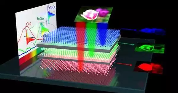
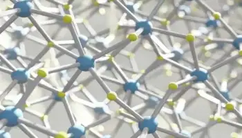
The van der Waals semiconductors enabled vertical color sensor (vdW-Ss) is a new class of materials in which individual atomic layers are held together by weak van der Waals forces. They are one of the most important platforms for discovering new physics and developing next-generation gadgets.
Because of their ultrathinness, mechanical flexibility, and chemical stability, these new semiconductor materials can be stacked in any order. So, in contrast to the present planar microelectronics layout, we are offering a three-dimensional integration technique. The increased integrated density is the primary reason why our device architecture can expedite camera downscaling, “Li explains.
The technology is currently patent pending with Georgia State University’s Office of Technology Transfer and Commercialization (OTTC). OTTC thinks that some industry partners will be very interested in this new design. “This technology has the potential to address some of the major disadvantages encountered with current sensors,” says Cliff Michaels, Director of OTTC. “As nanotechnology improves and devices become smaller, these smaller, highly sensitive color sensors will become extremely helpful.”
Researchers hope the discovery could lead to breakthroughs in helping the blind and visually handicapped in the future.
“This technology is essential for the development of biomimetic electronic eyes as well as other neuromorphic prosthetic devices,” Li explains. “In the future, high-quality color sensing and picture recognition functions may open up new avenues of colorful object perception for the visually impaired.”
According to Lei, his team will use what they’ve learned from this discovery to continue pushing these advanced technologies forward.
“This is a significant step forward, but there are still scientific and technical difficulties ahead, such as wafer-scale integration. Commercial image sensors can incorporate millions of pixels to provide high-definition images, but this has yet to be implemented in our prototype, “he claims. This large-scale van der Waals semiconductor device integration is currently a crucial problem that the entire scientific community must overcome. In collaboration with our colleagues at the Oak Ridge National Laboratory, that is where our team is focusing its efforts.

