In a review that affirms its commitment as the leading edge semiconductor material, UC St. Barbara scientists have straightforwardly pictured the photocarrier transport properties of cubic boron arsenide single gems.
“We had the option to picture how the charge moves in our example,” said Bolin Liao, an associate teacher of mechanical design in the School of Designing. Utilizing the main checking ultrafast electron microscopy (SUEM) arrangement in activity at a U.S. college, he and his group had the option to make “films” of the age and transport cycles of a photoexcited charge in this somewhat little-concentrated III-V semiconductor material, which has as of late been perceived as having uncommon electrical and thermal properties. All the while, they tracked down one more useful property that adds to the material’s true capacity as the following incredible semiconductor.
Their exploration, led as a team by material science teacher Zhifeng Ren’s gathering at the College of Houston, who’s work in creating great single gems of cubic boron arsenide, shows up in the journal Matter.
“Ringing the chime”
Boron arsenide is being looked at as a likely contender to supplant silicon, the PC world’s staple semiconductor material, because of its promising exhibit. For a certain something, with a better charge portability over silicon, it effectively leads current (electrons and their decidedly charged partner, “openings”). Nonetheless, unlike silicon, it likewise leads to heat easily.
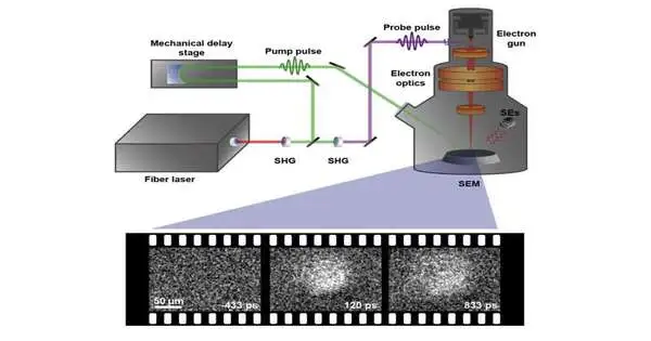
“We combine this incredibly high spatial resolution with an ultrafast laser, which functions as a very rapid shutter, to get exceptionally high time resolution. We’re talking about a picosecond, which is one millionth of a millionth of a second. As a result, we can film these minuscule energy and charge transport processes.”
Bolin Liao, an assistant professor of mechanical engineering in the College of Engineering.
“This material really has multiple times higher warm conductivity than silicon,” Liao said. This intensity leading—and delivering—capacity is especially significant as electronic parts become more modest and more thickly stuffed, and pooled heat undermines the gadgets’ exhibition, he made sense of.
“As your cellphones become more remarkable, you need to have the option to scatter the intensity. In any case, you have proficiency and security issues,” he said. “Warm administration has been difficult for a ton of microelectronic gadgets.”
What leads to the high warm conductivity of this material, it turns out, can likewise prompt fascinating vehicle properties of photocarriers, which are the charges energized by light, for instance, in a sun-based cell. Assuming it is tentatively checked, this would show that cubic boron arsenide can likewise be a promising material for photovoltaic and light location applications. Direct estimation of photocarrier transport in cubic boron arsenide, nonetheless, has been difficult because of the small size of accessible great examples.
The examination group’s review joins two accomplishments: the gem development abilities of the College of Houston group and the imaging abilities at UC St. Nick’s. Combining the capacities of the checking electron magnifying lens and femtosecond ultrafast lasers, the UCSB group assembled what is basically a very quick, incredibly high-goal camera.
“Electron magnifying lenses have awesome spatial goals — they can determine single iotas with their sub-nanometer spatial goal — yet they’re commonly sluggish,” Liao said, noticing this makes them great for catching static pictures.
“With our method, we couple this high spatial goal with an ultrafast laser, which goes about as fast as a quick shade, for a very high time goal,” Liao explained. “We’re discussing one picosecond — a millionth of a millionth of a second. So we can make films of these tiny energy and charge transport processes. ” Initially created at Caltech, the strategy was additionally evolved and improved at UCSB without any preparation and is currently the only functional SUEM arrangement at an American college.
“What happens is that we have one heartbeat of this laser that energizes the example,” made sense to graduate understudy analyst Usama Choudhry, the lead creator of the Matter paper. “You can imagine it like ringing a bell; a noisy clamor gradually lessens over the long run.” As they “ring the chime,” he made sense of, a subsequent laser beat is engaged on a photocathode (“electron weapon”) to create a short electron heartbeat to picture the example. They then check the electron beat after some time to acquire a full image of the ring. “By simply taking a ton of these sweeps, you can get a film of how the electrons and holes get energized and at last return to typical,” he said.
Among the things they saw while energizing their example and watching the electrons return to their unique state is the way the “hot” electrons endure.
“We found, shockingly, that the ‘hot’ electrons energized by light in this material can endure many more times than in regular semiconductors,” Liao said. These “hot” transporters supposedly persisted for an additional 200 picoseconds, a property that is connected with the very inclusion that is liable for the material’s high warm conductivity. This capacity to have “hot” electrons for altogether longer measures of time has significant ramifications.
For instance, when you energize the electrons in a common sun-based cell with light, few out of every odd electron have a similar measure of energy, “Choudhry made sense of. “The high-energy electrons have a short lifetime, and the low-energy electrons have an extremely lengthy lifetime.” With regards to reaping the energy from a common sun-based cell, he said, only the low-energy electrons are effectively being gathered; the high-energy ones will generally lose their energy quickly as intensity. Due to the ingenuity of the great energy transporters, in the event that this material was utilized as a sun-based cell, more energy could effectively be reaped from it.
With boron arsenide beating silicon in three pertinent regions — charge portability, warm conductivity, and hot photocarrier transport time — it can possibly turn into the gadget world’s next cutting-edge material. In any case, it actually faces huge obstacles—the creation of great gems in huge amounts—before it can rival silicon, colossal measures of which can be made somewhat efficiently and of top caliber. Yet, Liao doesn’t see an over the top issue.
“Silicon is currently regularly accessible due to long periods of venture; individuals began creating silicon around the 1930s and ’40s,” he said. “I think once individuals perceive the capability of this material, there will be more exertion put into tracking down ways of developing and using it. UCSB is very situated for this test in areas of strength for semiconductor improvement. “
More information: Usama Choudhry et al, Persistent hot carrier diffusion in boron arsenide single crystals imaged by ultrafast electron microscopy, Matter (2022). DOI: 10.1016/j.matt.2022.09.029
Journal information: Matter


