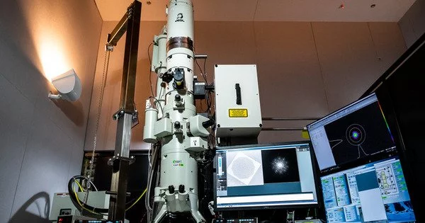
A team of researchers from Nagoya University in Japan used a novel combination of technologies to investigate the mechanisms of light-matter interaction in nanomaterials at the smallest and fastest scales.
Nanomaterials, or materials with nanoscale dimensions ranging from 1 to 100 nm, are becoming increasingly important in industry and daily life. Because of their extremely small size, they have unique properties that are not found in larger materials. These properties are also unique to the material’s nature and environment. To increase the number of nanomaterials that can be used effectively, safely, and sustainably in products and manufacturing processes, we need a better understanding of even the smallest events that occur on and inside nanoparticles.
To measure nanomaterials, scientists use a subfield of metrology known as nanometrology. Nanometrology measures length scales at the nanoscale. To give this some context, a human hair is about 100,000 times wider. When particles are this small, scientists must also measure events that occur within mere fractions of a second. For example, a phenomenon called photoexcitation normally takes place in picoseconds, or one trillionth of a second. Specialized devices, therefore, are necessary to measure these almost instantaneous events.
We expect this achievement to enable the analysis of photoelectric and thermoelectric conversion materials and their applied devices that contribute to energy conservation. Our research should be useful for the development of light energy conversion, biosensors, and thermoelectric conversion devices.
Makoto Kuwahara
A research group led by Nagoya University faculty members, Associate Professor Makoto Kuwahara from the Institute of Materials and Systems for Sustainability (IMaSS) and Lira Mizuno, Rina Yokoi, and Hideo Morishita of the Graduate School of Engineering, investigated whether they could study such photoexcitation processes occurring on single nanoparticles.
In collaboration with senior researchers at Hitachi Hightech Ltd., they developed an ultrafast electron microscope by combining a semiconductor photocathode with a ‘Negative Electron Affinity’ surface, pioneered by Nagoya University, with a general-purpose electron microscope. With the resulting microscope created by combining these technologies, we can observe events at the nanoscale. The researchers published their findings in Applied Physics Letters.
For the nanoparticles, the group used chemically synthesized gold nanotriangles. Gold is suitable for such experiments because it is a noble metal. This means it is stable under a range of conditions. Electrons in gold nanoparticles exhibit a phenomenon called ‘plasmon resonance’.
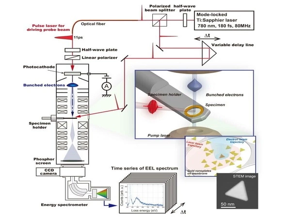
When a gold nanoparticle undergoes photoexcitation with a specific wavelength of light, the electrons in the nanoparticle start moving, or oscillating. This intensifies the light, turning the gold nanoparticle into a bright antenna. For this reason, surface plasmons on gold are regularly used for sensing applications and are of great interest in energy conversion.
The plasmons in gold nanoparticles can be photoexcited using the ultrafast laser in the new custom-built ultrafast electron microscope while simultaneously allowing scientists to observe single gold nanoparticles. The researchers investigated two different plasmon phenomena by applying their new technique.
They first observed the relaxation of the plasmons on the surface, which is a well-studied process. However, their new technique also allowed them to view the change in the plasmons inside the gold nanoparticles, even though the light only reached the surface of the nanoparticles.
This is the first time a technique has revealed the relaxation process of these plasmons inside the gold nanoparticles, with important implications for the preparation of light-harvesting materials for energy conversion. The newly developed technique should help analyze potential materials by exposing ultrafast light-matter interactions.
“By understanding phenomena such as photoexcitation and relaxation processes and energy transport, we can improve photoresponsive properties and increase efficiency,” explains Kuwahara.
“In particular, it can be a powerful tool to capture individual time changes in small structural materials with spatial resolution (such as those that exceed sub-micrometers). This has been difficult to achieve with conventional analytical methods using pulsed lasers as probes,” he continued.
“We expect this achievement to enable the analysis of photoelectric and thermoelectric conversion materials and their applied devices that contribute to energy conservation. Our research should be useful for the development of light energy conversion, biosensors, and thermoelectric conversion devices.”
