Your telephone might have in excess of 15 billion little semiconductors stuffed into its microchip chips. The semiconductors are made of silicon, metals like gold and copper, and protectors that together take an electric flow and convert it to 1s and 0s to impart data and store it. The semiconductor materials are inorganic, essentially derived from rock and metal.
Be that as it may, imagine a scenario in which you could make these crucial electronic parts part of nature, ready to respond straightforwardly to climate change like living tissue.
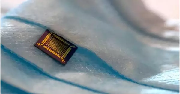
This is the very thing that a group at Tufts College Silklab did when they made semiconductors, supplanting the protective material with natural silk. They detailed their discoveries in cutting-edge materials.
Silk fibroin—the primary protein of silk strands—can be precisely kept on surfaces and handily altered with other compounds and organic atoms to change its properties. Silk, functionalized as such, can distinguish a large number of parts from the body or climate.
“Imagine making circuits that use information that isn’t represented by the discrete binary levels used in digital computing, but can process variable information like in analog computing, with the variation caused by changing what’s inside the silk insulator.”
led by Fiorenzo Omenetto,
The group’s most memorable exhibit of a model gadget utilized half-and-half semiconductors with silk fibroin to make a profoundly delicate and ultrafast breath sensor, identifying changes in mugginess.
Further alterations of the silk layer in the semiconductors could empower gadgets to distinguish a few cardiovascular and pneumonic illnesses, as well as rest apnea, or get carbon dioxide levels and different gases and particles in the breath that could give symptomatic data. Utilized with blood plasma, they might actually give data on degrees of oxygenation and glucose, coursing antibodies, and that’s just the beginning.
Before the advancement of the half and half semiconductors, the Silklab, driven by Fiorenzo Omenetto, the Honest C. Doble Teacher of Design, had previously utilized fibroin to create bioactive inks for textures that can distinguish changes in the climate or on the body, detecting tattoos that can be put under the skin or on the teeth to screen wellbeing and diet, and sensors that can be imprinted on any surface to recognize microbes like the infection answerable for Coronavirus.
How it functions
A semiconductor is just an electrical switch, with one metal electrical lead coming in and another going out. In the middle of the leads is the semiconductor material, which is supposed to be there on the grounds that it’s not ready to direct power except if cajoled.
One more wellspring of electrical information called a door is isolated from all the other things by a protector. The door acts as the “key” to turn the semiconductor on and off. It sets off the on-state when a limit voltage creates an electric field across the protector, preparing electron development in the semiconductor and beginning the progression of flow through the leads.
In a natural cross-breed semiconductor, a silk layer is utilized as the encasing, and when it retains dampness, it behaves like a gel, conveying whatever particles (electrically charged particles) are held inside. The door sets off the on-state by modifying particles in the silk gel. By changing the ionic creation in the silk, the semiconductor activity changes, permitting it to be set off by any entryway value somewhere in the range of nothing and one.
“You could envision making circuits that utilize data that isn’t addressed by the discrete paired levels utilized in computerized figuring but can handle variable data as in simple registering, with the variety brought about by changing what’s inside the silk cover,” said Omenetto. “This opens up the chance of bringing science into figuring out the inside of the current chip.” Obviously, the most impressive natural PC is the cerebrum, which processes data with variable degrees of compound and electrical signs.
The specialized test in making half-breed natural semiconductors was to accomplish silk handling at the nanoscale, down to 10 nm, or under 1/10,000th the width of a human hair.
“Having accomplished that, we can now make half-and-half semiconductors with similar creation processes that are utilized for business chip production,” said Beom Joon Kim, a postdoctoral specialist at the School of Designing. “This implies you can make a billion of these with capacities accessible today.”
Having billions of semiconductor hubs with associations reconfigured by organic cycles in the silk could prompt chips that could carry on like the brain networks utilized in computer-based intelligence. “Looking forward, one could envision having coordinated circuits that train themselves, answer ecological signals, and record memory straightforwardly in the semiconductors as opposed to sending it to isolate capacity,” said Omenetto.
Gadgets for identifying and answering more complicated natural states, as well as huge-scope simple and neuromorphic processing, are yet to be made. Omenetto is hopeful about future open doors. “This opens up a better approach for pondering the point of interaction among hardware and science, with numerous significant and crucial revelations and applications ahead.”
More information: Beom Joon Kim et al, Bimodal Gating Mechanism in Hybrid Thin‐Film Transistors Based on Dynamically Reconfigurable Nanoscale Biopolymer Interfaces, Advanced Materials (2023). DOI: 10.1002/adma.202302062


