Specialists at Tohoku College have created rules for a solitary nanometer attractive passage intersection (MTJ), considering execution fitting to meet the prerequisites of different applications, going from computer-based intelligence (IoT) to cars and space innovations.
The advanced will prompt elite execution of spintronic non-unstable memory, viable with cutting-edge semiconductor innovations. The subtleties were distributed in the diary of npj Spintronics on January 4, 2024.
The vital quality of non-unstable memory is its capacity to hold information without even a trace of an outer power source. Subsequently, broad improvement endeavors have been coordinated towards non-unstable memory on account of its capacity to diminish power utilization in semiconductor-coordinated circuits (ICs). Execution necessities for non-unpredictable memory change as per explicit applications. For example, man-made intelligence and IoT applications request rapid execution, while auto and space advancements focus on high maintenance capacities.
“Because the proposed structure may be adapted to existing facilities in large semiconductor manufacturers, we feel that our study provides a significant contribution to the future scaling of STT-MRAM,”
Junta Igarashi, one of the lead authors of the study.
Turn-move force magnetoresistive irregular access memory (STT-MRAM), a kind of non-unstable memory innovation that stores information by using the inherent rakish energy of electrons, known as twist, has the possibility to address a portion of the limits related to existing memory innovations.
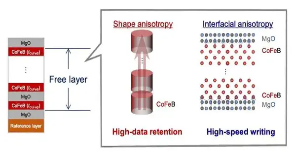
The fundamental structure block of STT-MRAM is the attractive passage intersection (MTJ): two ferromagnetic layers isolated by a slight protective boundary. Researchers have long attempted to address the difficulty of making MTJs more modest while meeting execution prerequisites; however, numerous issues remain.
STT-MRAM, utilizing MTJs with aspects in the scope of many nanometers, has been effectively produced for car semiconductors utilizing 1X nm innovation hubs. Looking forward to future hubs, notwithstanding, there is a need to downsize MTJs to single-digit nanometers, or X nm, while guaranteeing the capacity to fit execution as per explicit applications.
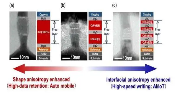
Cross-sectional transmission electron magnifying lens pictures of the manufactured MTJs and their film stacks. Shifting the quantity of CoFeB/MgO layers and the CoFeB thickness can fit MTJ execution for maintenance-basic to speed-basic applications. Credit: Junta Igarashi, Butsurin Jinnai, and Shunsuke Fukami. From npj Spintronics (2024). DOI: 10.1038/s44306-023-00003-2
To do this, the examination bunch planned a way to design single-nanometer MTJs with a CoFeB/MgO stack structure, a true standard material framework. Fluctuating the individual CoFeB layer thickness and the quantity of [CoFeB/MgO] stacks permitted them to control the shape and interfacial anisotropies autonomously—something pivotal for accomplishing high maintenance and high velocity capacities separately.
Subsequently, the MTJ execution can be customized for applications going from maintenance-basic to speed-basic. At the size of single nanometers, shape-anisotropy-improved MTJs showed high maintenance (> 10 years) at 150°C, while interfacial-anisotropy-improved MTJs accomplished quick speed exchanging (10 ns or more) under 1 V.
“Since the proposed construction can be adjusted to existing offices in significant semiconductor processing plants, we accept that our review gives a critical commitment to the future scaling of STT-MRAM,” said Junta Igarashi, one of the lead creators of the review.
Head Agent Shunsuke Fukami added that “semiconductor enterprises will commonly be aware of dependable scaling. In that sense, I figure this work ought to send major areas of strength to them so that they can depend on the fate of STT-MRAM to assist with introducing a low-carbon society.”
More information: Junta Igarashi et al, Single-nanometer CoFeB/MgO magnetic tunnel junctions with high retention and high-speed capabilities, npj Spintronics (2024). DOI: 10.1038/s44306-023-00003-2


