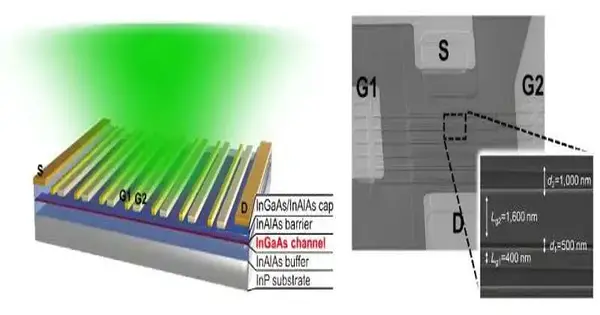
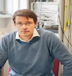
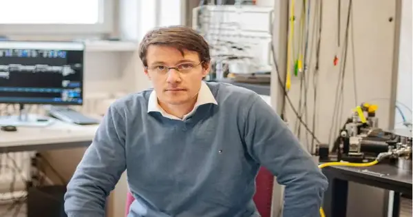
close

Nanophysics

Nanophysics

Thermal magIC: Investigating the inner workings of an ambitious new ‘thermometry camera’

Thermometers can do a great deal of things: measure the temperature at the focal point of your impeccably braised chicken, or let you know whether to keep your kid home from school because of sickness. But because of their size, conventional thermometers' purposes are as yet restricted. "How would you painlessly measure a temperature inside a living framework like a human?" said NIST's Thinh Bui. "Or, on the other hand, in different conditions that might be difficult to get to—say, the temperature inside a Kevlar vest as a shot enters it. How would you approach that? You can't put a
Nanophysics

A technique for 3D printing metals at the nanoscale provides an unexpected benefit.

Before the end of last year, Caltech specialists uncovered that they had fostered another manufacturing method for printing micro sized metal parts containing highlights probably as thick as three or four pieces of paper. Presently, the group has reexamined the strategy to consider printing objects multiple times more modest: 150 nanometers, which is practically identical to the size of a seasonal infection. In doing so, the group additionally found that the nuclear game plans inside these articles are confused, which would, on a large scale, make these materials unusable in light of the fact that they would be viewed as
Nanophysics

An atomic layer deposition method to scalable, electronic-grade van der Waals tellurium thin films is demonstrated in this study.

An exploration group, led by Teacher Joonki Suh in the Branch of Materials Science and Designing and the Doctoral-level College of Semiconductor Materials and Gadgets Designing at UNIST, has made a huge leap in slender film statement innovation. By utilizing an inventive nuclear layer statement (ALD) process, teacher website optimization effectively accomplished the customary course of action of tellurium (Te) particles at low temperatures as low as 50 degrees Celsius. The ALD technique is a state-of-the art slim film process that empowers exact stacking of semiconductor materials at the nuclear layer level on three-layered structures—even at low interaction temperatures. In
Nanophysics

Subsurface nanometrology: Using atomic force microscopy to investigate buried materials

A new nanoscience concentration driven by a specialist at the Branch of Energy's Oak Edge Public Research Facility takes a 10,000-foot view to take a gander at how researchers concentrate on materials at the littlest scales. The paper, distributed in Science Advances, surveys driving work in subsurface nanometrology, the study of inner estimation at the nanoscale level, and proposes quantum detecting could turn into the establishment for the field's next time of disclosures. Potential applications could range from planning intracellular designs for designated drug conveyance to describing quantum materials and nanostructures for quantum registering. "Our objective was to characterize the
Nanophysics

Developing beyond-silicon technology using residue-free field effect transistors

An unrest in innovation is not too far off, and it's ready to change the gadgets that we use. Under the initiative of Teacher Lee Youthful Hee, a group of specialists from the Middle for Incorporated Nanostructure Physical Science inside the Establishment for Essential Science (IBS), South Korea, has disclosed another disclosure that can have an incredible impact on the manufacture of field-impact semiconductors (FET). Their examination is distributed in Nature Nanotechnology. A superior field-impact semiconductor (FET) is a fundamental structure block for cutting-edge silicon-based semiconductor innovations. Current 3-layered silicon innovation experiences debasement of FET exhibitions when the gadget is
Nanophysics

Quantum matter shows ‘non-local’ behavior similar to brain function.

We frequently accept that PCs are more proficient than people. All things considered, PCs can finish a mind-boggling numerical statement in a second and can likewise review the name of that one entertainer we continue neglecting. In any case, human cerebrums can handle convoluted layers of data rapidly, precisely, and with practically no energy input, such as perceiving a face after just seeing it once or quickly knowing the contrast between a mountain and the sea. These straightforward human errands require tremendous handling and energy input from PCs, and, surprisingly, at that point, with fluctuating levels of exactness. Making minds
Nanophysics

Researchers believe they have overcome the’mirror twins’ problem that has plagued the next generation of 2D semiconductors.

The up-and-coming age of 2D semiconductor materials could do without what it sees when it thoroughly searches in the mirror. Current orchestrating ways to make single-layer nanosheets of semiconducting material for molecularly meager hardware create a particular "reflect twin" imperfection when the material is kept on single-gem substrates like sapphire. The blended nanosheet contains grain limits that go about as a mirror, with the game plan of particles on each side coordinated in reflected resistance to each other. This is an issue, as indicated by specialists from Penn State's Two-Layer Gem Consortium-Materials Development Stage (2DCC-MIP) and their colleagues. Electrons disperse
Nanophysics

Using rainbow scattering to learn more about graphene

Graphene is a two-layered wonder material that has been proposed for a great many applications in energy, innovation, development, and more since it was first secluded from graphite in 2004. This single layer of carbon molecules is intense yet adaptable, light yet with high opposition, with graphene determined to be multiple times more safe than steel and multiple times lighter than aluminum. Graphene might sound great, yet it in a real sense isn't. Disengaged tests of this 2D allotrope aren't completely level, with its surface undulated. Graphene can likewise highlight primary imperfections that can, at times, be malicious to its
Nanophysics

Highlighting an ‘innovative approach’ to 2D material research

A new exploration from Lancaster College presents a "creative methodology" for researching the intensity conductivity of novel two-layered materials. The work makes ready for making proficient waste intensity scroungers that create modest power, new reduced refrigerators, and progressed optical and microwave sensors and cameras. The examination, driven by Teacher of Nanoscience Oleg Kolosov and Ph.D. understudy Sergio Gonzalez-Munoz, straightforwardly gauges the intensity conductivity of two-layered materials (2DMs). The journal Advanced Materials Interfaces has published it. The weaker van der Waals forces connect stacks of nearly perfect, tightly bound atomic sheets that make up two-dimensional materials. Recent discoveries like graphene, molybdenum
Nanophysics

The new process for forming liquid metal nanodroplets has interesting catalytic capabilities.

A new method developed at Australia's RMIT University has resulted in the successful formation of liquid metal nanodroplets with the appearance of planets. Like our own planet Earth, the nanodroplets include an external "outside layer," a fluid metal "mantle," and a strong "center." The strong intermetallic center is the way to accomplish a more homogenous blend by "securing" a similar measure of solute (i.e., the "target" metals) in each alloyed drop. The examination group achieved homogeneity through complete disintegration inside the fluid metal medium, made conceivable by high-temperature liquid salt. Their article, "Combination of planet-like fluid metal nanodroplets with promising