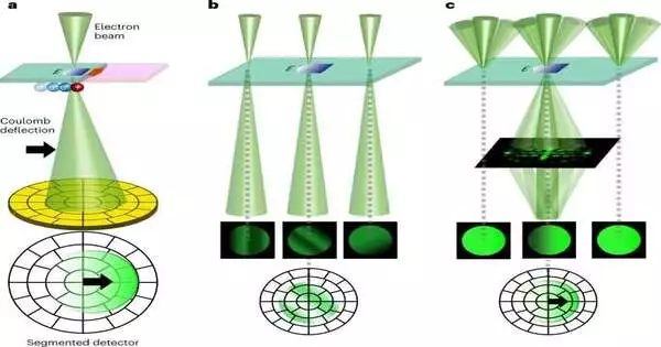
The University of Tokyo team, under the direction of Professor Naoya Shibata, worked with Sony Group Corporation to successfully observe up close a two-dimensional electron gas that had gathered at the semiconductor interface. Highly effective light-emitting diodes (LEDs) and laser diodes (LDs) are made from GaN-based components. These are anticipated to be used as next-generation high-frequency devices for communication as well as power devices for power conversion due to their high dielectric breakdown strength and saturated electron velocity. A layer of accumulated electrons known as a two-dimensional electron gas is produced at the semiconductor interface, specifically by high-electron-mobility transistors (HEMTs).
Nanotechnology
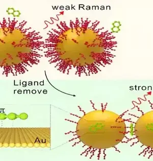
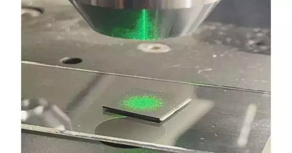
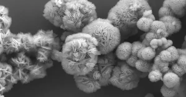
Surface-enhanced Raman scattering (or spectroscopy), also known as SERS, is a sophisticated analysis technique that expands the scope of Raman applications to include trace analysis, such as the detection of a pollutant at the part-per-million level in water or other liquids. Biochemistry, forensics, food safety, threat detection, and medical diagnostics are all potential applications for SERS. However, inexpensive and dependable SERS substrates that permit reproducible spectral signals are still required before the method can be utilized in clinical and industrial settings. By creating a new substrate with plasmonic and photocatalytic nanostructures, material scientists from Kiel University advanced the SERS method.
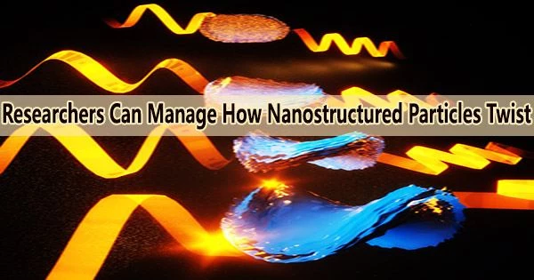
A research team lead by the University of Michigan has demonstrated that micron-sized “bow ties,” self-assembled from nanoparticles, generate a range of distinct curling shapes that can be precisely controlled. The discovery makes it possible to produce materials that interact with twisted light with ease, as well as new machine vision tools and pharmaceuticals. While chiral structures, such as DNA, are abundant in life, their degree of twist cannot be changed without the structure breaking. Now, researchers can engineer the degree of twist. Such materials could enable robots to accurately navigate complex human environments. Instead of the 2D arrangement of
The key to a perfect croissant is the number of layers, as many as possible, and the addition of butter to each one.In a similar vein, scientists are able to slip various ions between a number of extremely thin metal layers in a novel material that holds promise for novel applications. As a result, energy storage and high-tech electronics could benefit greatly from their use in the future. These materials, which are pronounced "max-eens" and are referred to as MXenes, were previously as labor-intensive as good croissants made in a French bakery. However, a new method developed by researchers at
According to a study published in the journal Molecular Therapy, newly developed mRNA vaccines against HIV-1 and Zika virus generated robust antibody responses that were passed on from pregnant rabbits to their offspring. The findings, as noted by the authors, support the development of their vaccine platform, LION/repRNA, for use in maternal and neonatal settings to prevent the transmission of pathogens from mother to child in both animals and humans. The development of mRNA vaccines for other infectious diseases will be sparked by the recent success of mRNA vaccines against the COVID-19 pandemic. mRNA vaccines have been approved by the
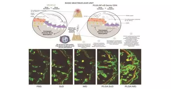
Is there a regenerative medicine "magic bullet"? A cutting-edge gene therapy for repairing tissues damaged by disease or trauma has long been a goal of scientists. Now that a research team has created a polymeric gene delivery therapy that encourages new bone formation following traumatic inflammation, that wish may come true. Researchers from Tokyo Medical and Dental University (TMDU) discovered in a study that was published in the International Journal of Molecular Sciences that a gene delivery therapy can effectively reduce inflammation and speed up tissue healing following tooth extraction. Tooth extraction is a common procedure in dental medicine.Sores form
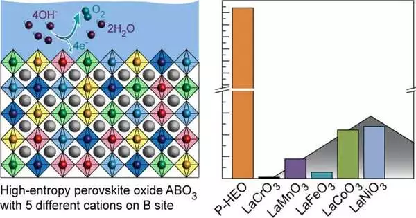
A new composite material that outperforms individual compounds by one to two orders of magnitude was created by University of Twente researchers. Several earth-abundant elements make up the composite, which could potentially be used to produce hydrogen efficiently without platinum or other precious or rare metals. The findings were presented by the researchers in the journal ACS Nano. The energy carrier of the future is thought to be green hydrogen. In essence, hydrogen provides a means of storing (green) energy for extended periods of time. Because of this, it is of the utmost significance to produce it as quickly as
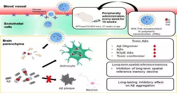
Some of the time the best things in life happen by coincidence, when we end up being perfectly located. Presently, scientists from Japan have figured out how to guarantee that new drugs are conveyed to the perfect locations in the body at the ideal timepoint in sickness movement, so they make the best difference. In a review distributed as of late in the Journal of Nanobiotechnology, scientists driven by the Tokyo Clinical and Dental College (TMDU) have uncovered that a clever conveyance framework conveys treatment to where it is needed most in a mouse model of Alzheimer's disease (Promotion). Promotion
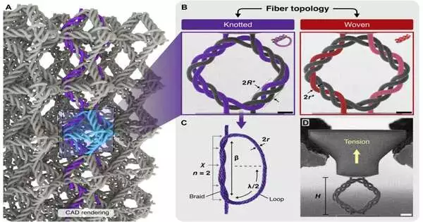
In the most recent development in nano- and miniature-architected materials, engineers at Caltech have fostered another material produced using various interconnected microscale hits. The bunches make the material far harder than indistinguishably organized but unknotted materials: they retain more energy and can twist more while still having the option to get back to their unique shape. These new hitching materials might find applications in biomedicine as well as in aviation applications because of their toughness, conceivable biocompatibility, and outrageous deformability. "The capacity to defeat the general compromise between material deformability and elastic strength offers better approaches to designing gadgets that
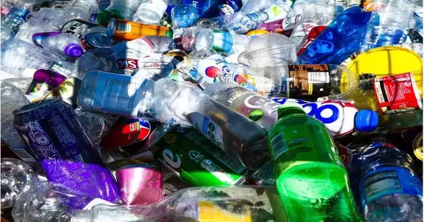
A group of scientists at NYU Abu Dhabi has fostered a solitary step, natural dissolvable free, aqueous cycle to change over polyethylene-based plastic sacks and polypropylene-based careful veils into carbon dabs. An expected 26,000 metric tons of pandemic-related plastic waste — from clinical waste to internet shopping bundling — have been delivered into the world's seas, making it much more dire to track down effective techniques to upcycle this non-degradable material. One arrangement is to change over the single-use plastic into alleged carbon dabs, carbon nanomaterials that are biocompatible and have applications in the fields of organic imaging, natural checking,
