close

Nanotechnology

Nanotechnology

Unique two-dimensional periodic surface nanostructures can be produced by femtosecond laser pulses operating in GHz burst mode.

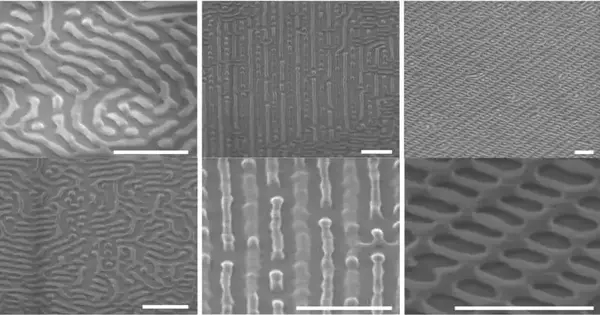
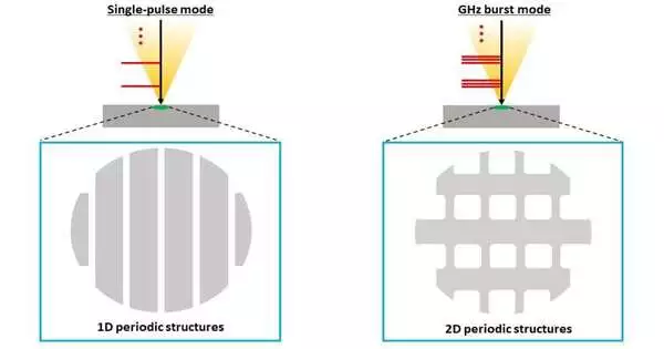
Researchers dealing with laser application at the RIKEN Community for Cutting Edge Photonics (RAP) have shown that GHz burst mode femtosecond laser heartbeats can make interesting two-layered (2D) laser-incited intermittent surface designs (LIPSS) on silicon substrates. Previously, a group led by scientists from the High Level Laser Handling Exploration Group detailed that GHz burst mode femtosecond laser beats, which consist of a series of trains of ultrashort laser beats with a heartbeat time frame of hundred picoseconds (ps), significantly improve removal proficiency and quality when compared to ordinary femtosecond laser handling (single-beat mode). Distributed in the International Journal of Extraordinary
Nanotechnology

Study links daily force’s nano- and macro-aspects

Without the power of contact, vehicles would slip off the street, people couldn't walk down the walkway, and items would tumble off your kitchen counter and onto the floor. All things being equal, how rubbing works at a sub-atomic scale remains inadequately comprehended. A team led by a postdoctoral scientist at Johns Hopkins Whiting School of Design and Krieger Institute of Expressions and Sciences used complex displaying and virtual experiences to focus on contact at both the subatomic and plainly visible scales.The group's review findings, which appear in ACS Nano, shed light on rubbing in general, but could also illuminate
Nanotechnology

Rust-busting technology brings recyclable mobile phone batteries one step closer.

Cell phone batteries with a lifetime up to quite a bit longer than the present innovation could be a reality because of a development drove by engineers at RMIT College. Instead of discarding batteries following a few years, we could have recyclable batteries that keep going for as long as nine years, the group says, by utilizing high-recurrence sound waves to eliminate rust that hinders battery execution. The exploration is distributed in Nature Correspondences. Just 10% of utilized handheld batteries, including for cell phones, are gathered for reusing in Australia, which is low by global norms. The excess 90% of
Nanotechnology

New insights regarding the use of nanotechnology-based pharmaceuticals

Novel medications, like antibodies against Coronavirus, among others, depend on drug transport utilizing nanoparticles. Whether this medication's transport is harmed by a gathering of blood proteins on the nanoparticle's surface was not explained for quite a while. The Max Planck Foundation for Polymer Exploration has now followed the path of such a molecule into a cell using a combination of microscopy techniques.They had the option to notice a cell-inner cycle that really isolates blood parts and nanoparticles. Nanoparticles are a field of exploration, and imagining current medication without them is unthinkable. They act as tiny medication cases that are under
Nanotechnology

On industrial silicon wafers, scientists create ‘perfect’ atom-thin materials.

Consistent with Moore's Law, the quantity of semiconductors on a microprocessor has multiplied consistently since the 1960s. In any case, this direction is anticipated to soon reach a certain level since silicon, the foundation of current semiconductors, loses its electrical properties once gadgets produced using this material plunge below a certain size. Enter 2D materials: sensitive, two-layered sheets of wonderful gems that are essentially as meager as a solitary particle. At the size of nanometers, 2D materials can definitely direct electrons more productively than silicon. The quest for cutting-edge semiconductor materials in this manner has zeroed in on 2D materials
Nanotechnology

DNA is used as ‘bait’ in a highly accurate test for common respiratory viruses.

For quite a long time, semiconductors—tthe core of microchips—hhave been getting more and more modest. Accordingly, the electronic parts in numerous gadgets can be made much smaller, quicker, and, furthermore, more impressive. Be that as it may, is this improvement coming to a characteristic end? The more modest the parts, the more prominent the peril that singular imperfections in the nuclear construction will fundamentally change the way the part behaves. This applies to the laid-out silicon innovation and novel nanotechnologies in view of 2D materials. At the Vienna College of Innovation (TU Wien), serious work has been completed on the
Nanotechnology

Chemists create a novel type of nanomaterial.

There's a new nanomaterial on the block. A college of Oregon's scientific experts have figured out how to make carbon-based particles with a one-of-a kind underlying element: interlocking rings. Like other nanomaterials, these connected particles have intriguing properties that can be "tuned" by changing their size and composition. That makes them possibly valuable for a variety of uses, like specific sensors and new sorts of hardware. "It's another geography for carbon nanomaterials, and we're finding new properties that we haven't had the option to see previously," said James May, an alumni understudy in science teacher Ramesh Jasti's lab and the
Nanotechnology

New nanostructures are discovered through artificial intelligence.

Researchers at the U.S. Department of Energy's (DOE) Brookhaven Public Research Center have effectively shown the way that independent techniques can find new materials. The computerized reasoning (man-made intelligence)-driven method prompted the disclosure of three new nanostructures, including a first-of-its-kind nanoscale "stepping stool." The examination was distributed today in Science Advances. The newfound designs were framed by a cycle called "self-get together," in which a material's particles coordinate themselves into exceptional examples. Researchers at Brookhaven's Center for Utilitarian Nanomaterials (CFN) are seasoned veterans of coordinating the self-gathering process, making layouts for materials to frame beneficial plans for applications in microelectronics
Nanotechnology

A fresh approach to assessing thermoelectric materials

Working with one of the world's most transcendent thermoelectric materials scientists, a group of specialists in the Clemson Branch of Physical Science and Stargazing and the Clemson Nanomaterials Organization (CNI) has fostered a new, secure technique to assess thermoelectric materials. Division of Physical Science and Cosmology Exploration Aide Teacher Sriparna Bhattacharya, Architect Herbert Behlow, and CNI Establishing Chief Apparao Rao teamed up with incredibly famous analyst H. J. Goldsmid, teacher emeritus at the College of New South Wales (UNSW) in Sydney, Australia, to make a one-stop strategy for assessing the productivity of thermoelectric materials. Goldsmid is viewed by a lot
Nanotechnology

A study discovered that nickel nanowires improve microwave absorption.

In a review distributed in Cutting Edge Materials Connection Points, an examination group led by Prof. Wang Hui and partner Prof. Sheng Zhigao from the Hefei Foundations of Actual Science (HFIPS) of the Chinese Institute of Sciences detailed the union of polyvinylpyrrolidone-coordinated nickel nanowires (PNNWs) through a solvothermal strategy helped by a high attractive field and applied them to improve microwave retention. Among the many microwave safeguards that have been examined, one-layered attractive nanowires stand out due to their great mechanical properties, huge angle proportion, and superb electronic transmission execution. In any case, the smooth surface and lack of attraction