close

Nanotechnology

Nanotechnology

Scientists create 2D nanosheets for long-term carbon capture.

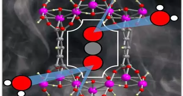
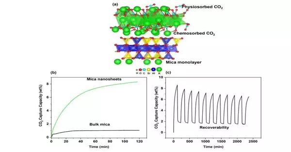
A dangerous atmospheric deviation has been credited to the sharp expansion in heat-catching ozone-depleting substance discharges, specifically CO2 outflows. A promising approach to reducing emissions is carbon capture technology, such as the utilization of adsorbents to capture and store CO2 from the surrounding air. Traditionally, liquid sorbents have been used to capture carbon, but their equipment corrosion, high cost, and high energy requirements for regeneration make them unsuitable. Solid porous materials for CO2 adsorption, in which CO2 atoms adhere to the surface of the solid material, are being investigated as a means of overcoming these limitations. In his carbon catch
Nanotechnology

Researchers develop a better method for capturing carbon from industrial pollutants.

An inexpensive nanomaterial has been shown to be capable of removing industrial emissions of carbon dioxide by researchers in the College of Science at Oregon State University. The discoveries, distributed in Cell Reports Actual Science, are significant on the grounds that better carbon capture strategies are a vital aspect of tending to environmental change, said OSU's Kyriakos Stylianou, who drove the review. Carbon dioxide, an ozone-depleting substance, comes about because of the consumption of petroleum products and is one of the essential drivers of a warming environment. "Carbon dioxide capture is critical for meeting net-zero emission targets, MOFs have shown
Nanotechnology

Nanotexture X-ray imaging is improved via machine learning

Researchers at Cornell used high-powered X-rays, phase-retrieval algorithms, and machine learning to reveal the intricate nanotextures in thin-film materials. This gave researchers a new, more efficient way to look at potential candidates for quantum computing and microelectronics, among other fields. Because they can impart novel properties to a material, nanotextures that are dispersed irregularly throughout a thin film are of particular interest to scientists. Visualizing the nanotextures directly is the most effective method for research, but this often necessitates complicated electron microscopy and does not preserve the sample. The new imaging procedure definite July 6 in the Procedures of the
Nanotechnology

AI-generated nanoparticles demonstrate their capacity to transport contemporary medications to ill cells.

Using artificial intelligence, researchers from Cardiff University and Astra Zeneca created microscopic particles that are able to effectively transport medicines to precisely target and treat diseased cells. The team says that their work could be used to treat genetic diseases, cancer, and infectious diseases in the future. The study was published in Small Methods under the title "Understanding intracellular biology to improve mRNA delivery by lipid nanoparticles." "We are constantly looking for new and improved ways of delivering drugs around the human body," stated Professor Arwyn T. Jones of Cardiff University's School of Pharmacy and Pharmaceutical Sciences. Nanoparticles are small
Nanotechnology

When used as a saturable absorber, graphene can produce two types of mode-locking states.

In order to generate mode-locked pulses, passive mode-locked technology regulates the loss and phase of the cavity by making use of the nonlinear absorption effect of saturable absorbers. Graphene has a very wide operating spectral range (300–2,500 nm), a low absorption coefficient, a significant modulation depth, and a unique energy bandgap structure. When it comes to fiber lasers' ultrashort pulse output, graphene has emerged as an ideal saturable absorber. Mode-locked pulses have been achieved by researchers in numerous graphene mode-locked technology experiments. According to patterns of energy distribution, laser pulses can also be divided into bright and dark pulses. Numerous
Nanotechnology

Researchers propose a new approach for directly fabricating sub-10-nm nanopores.

Using swift heavy ions, Chinese researchers have proposed a novel strategy for the direct fabrication of sub-10 nm nanopores in WO3 nanosheets. Nano Letters has published the findings. Researchers from the Joint Institute for Nuclear Research in Russia and the Materials Research Center of the Institute of Modern Physics (IMP) of the Chinese Academy of Sciences (CAS) collaborated on the study. For single-molecule detection, nanofluidic devices, and nanofiltration membranes, the production of high-quality solid-state nanopores is crucial. Focused ion or electron beams are the most common method for creating nanopores in SiN, Al2O3, and other inorganic films. However, this poring
Nanotechnology

A researcher uses a novel technology to 3D print the world’s smallest wineglass.

The world's smallest wine glass has a rim that is smaller than the width of a human hair and was 3D-printed by researchers. However, the objective was not to target extremely light drinkers. Instead, the glass was printed to show a new, easier way to make silica glass structures for everything from robotics to telecommunications. According to KTH Professor Frank Niklaus, the new method, which was developed at the Royal Institute of Technology in Stockholm, gets around issues like the need for thermal treatment when 3D-printing essential components made of silica glass. Nature Communications is the journal that published the
Nanotechnology

Researchers make significant progress toward developing an all-purpose biosensor chip.

Chip-based sensing devices that are utilized for the detection or analysis of substances have seen significant improvements from researchers. These accomplishments lay the groundwork for highly sensitive, portable, integrated optofluidic sensing devices that could be used to carry out a variety of medical tests simultaneously with completely different kinds of bioparticles—like DNA and viruses—at greatly varying concentrations. New signal processing methods were applied to an optofluidic chip-based biosensor by researchers led by Holger Schmidt from the W.M. Keck Center for Nanoscale Optofluidics at the University of California, Santa Cruz (UCSC), as reported in the journal Optica. The seamless fluorescence detection
Nanotechnology

A spectroscopic micro-ellipsometer has revealed atomic-level thickness measurements of two-dimensional materials.

Material flakes in two dimensions, or 2Ds, have extraordinary quantum properties that are not found in everyday materials because they are composed of just one or a few atomic layers. Consequently, these materials have enormous potential for advanced research and industrial applications. In the past, ellipsometry has been a popular optical method for measuring thin-film thicknesses without using any tools. However, 2D flakes frequently have lateral dimensions of only a few microns, and commercial ellipsometers are limited in their ability to measure areas smaller than 50–60 microns. A system and method for a microscope-integrated ellipsometer, known as the Spectroscopic Micro-Ellipsometer
Nanotechnology

The metasurface provides strong coupling effects between light and transition metal. dichalcogenides

Nanophotonics is all about how light and matter interact at the nanoscale. Scientists can control and improve electromagnetic energy in volumes smaller than the incident light's wavelength with resonant nanosystems. They not only make it possible to more effectively capture sunlight, but they also make it easier to better control emissions and optical wave guiding. In solid-state materials, the hybridized photonic and electronic states known as polaritons are produced by the strong coupling of light with electronic excitation. Polaritons can have fascinating properties like superfluidity and Bose-Einstein condensation. The nanoscale coupling of light and matter is making progress, according to