An exploration bunch from Tohoku College and RIKEN has fostered a high-velocity, high-responsiveness terahertz-wave finder working at room temperature, making ready for headways in the improvement of cutting-edge 6G/7G innovation.
Subtleties of their advancement were distributed in the journal Nanophotonics on November 9, 2023.
The upgrade of current interchange rates will depend on terahertz (THz) waves. THz waves are electromagnetic waves inside the THz range that fall between the microwave and infrared parts of the electromagnetic range, commonly spreading over frequencies from 300 gigahertz to 3 THz.
In any case, the quick and delicate discovery of THz waves at room temperature is trying for customary electronic- or photonic-based semiconductor gadgets.
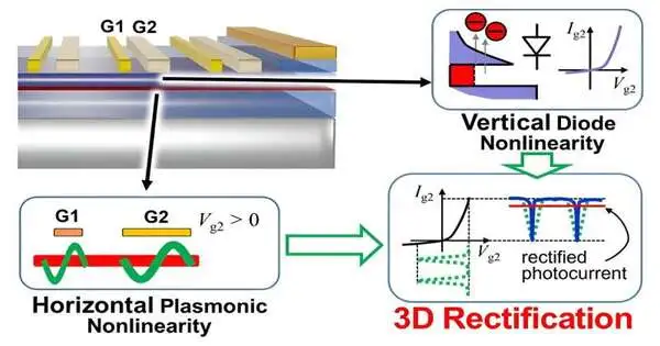
“We discovered a 3D plasmonic rectification effect in a THz wave detector based on an indium-phosphide high-electron mobility transistor, which allowed us to increase detection sensitivity by more than one order of magnitude over conventional detectors based on 2D plasmons.”
Akira Satou, leader of the research group and associate professor at Tohoku University’s Research Institute for Electrical Communication (RIEC).
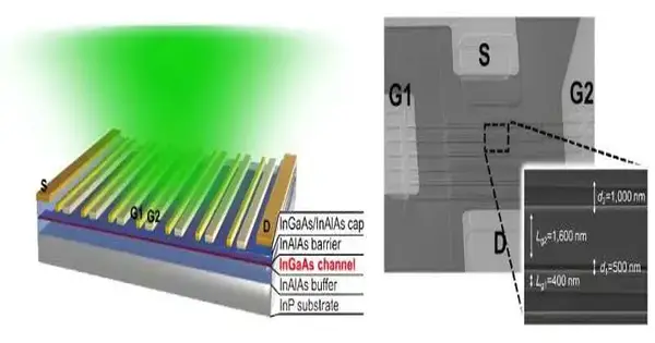
This is where two-layered plasmons come in. In a semiconductor field-impact semiconductor, there is a two-layered electron channel where aggregate charge-thickness quanta, i.e., two-layered plasmons, exist. These plasmons are energized conditions of electrons displaying liquid-like ways of behaving. Their nonlinear correction impacts, starting from these liquid-like ways of behaving, and their fast reaction (not compelled by electron travel time) make them a promising means to identify THz waves at room temperature.
Schematic perspective on the 3D correction impact on the gadget. Credit: Akira Satou et al
“We found a 3D plasmonic correction impact in the THz wave locator,” says Akira Satou, head of the examination gathering and academic partner at Tohoku College’s Exploration Organization for Electrical Correspondence (RIEC). “The indicator depended on an indium-phosphide high-electron portability semiconductor, and it empowered us to improve location awareness more than one significant degree higher than customary finders in view of 2D plasmons.”
The new discovery strategy consolidated the customary vertical hydrodynamic nonlinear correction impact of 2D plasmons with the expansion of an upward diode-current nonlinearity.
It likewise decisively settled the waveform mutilation brought about by various impressions of high-velocity tweaked signals—a basic issue in customary locators in view of 2D plasmons.
Driving the gathering close by Satou were Extraordinarily Selected Teacher Tetsuya Suemitsu from Tohoku College’s New Industry Creation Incubation Facility Center and Hiroaki Minamide from RIKEN Place for Cutting Edge Photonics.
“Our new recognition system defeats the vast majority of the bottlenecks in ordinary terahertz-wave locators,” adds Satou. “Looking forward, we desire to expand on our accomplishment by further developing the gadget execution.”
More information: Akira Satou et al. Gate-readout and a 3D rectification effect for giant responsivity enhancement of asymmetric dual-grating-gate plasmonic terahertz detectors, Nanophotonics (2023). DOI: 10.1515/nanoph-2023-0256


