Researchers, including an Oregon State College materials scientist, have fostered a superior device to gauge light, adding to a field known as optical spectrometry in a manner that could further develop everything from cell phone cameras to natural checking.
The review, distributed today in Science, was driven by Finland’s Aalto College and brought about a strong, super small spectrometer that fits on a CPU and works utilizing man-made reasoning.
The examination included a nearly new class of super-slim materials known as two-layered semiconductors, and the end result is a proof of concept for a spectrometer that could be promptly integrated into various innovations—including quality review stages, security sensors, biomedical analyzers, and space telescopes.
“We’ve shown an approach to building spectrometers that is undeniably smaller than what is normally utilized today,” said Ethan Minot, a teacher of physical science in the OSU School of Science. “Spectrometers measure the strength of light at various frequencies and are really helpful in heaps of ventures and all areas of science for recognizing tests and describing materials.”
“We developed a method for making spectrometers that are significantly more compact than what is now used. Spectrometers detect the intensity of light at different wavelengths and are extremely useful in a wide range of industries and scientific sectors for identifying samples and describing materials.”
Ethan Minot, a professor of physics in the OSU College of Science.
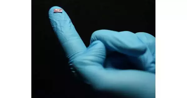
Minot said that conventional spectrometers require massive optical and mechanical parts, while the new gadget could fit on the end of a human hair. The new examination proposes those parts can be supplanted with novel semiconductor materials and man-made intelligence, permitting spectrometers to be decisively downsized in size from the current smallest ones, which are about the size of a grape.
“Our spectrometer doesn’t need to gather separate optical and mechanical parts or exhibit plans to scatter and channel light,” said Hoon Hahn Yoon, who led the review with Aalto College partner Zhipei Sun Yoon. Besides, it can accomplish a high goal similar to benchtop frameworks, yet in a lot more modest bundle.
According to the analysts, the device is 100 percent electrically controllable in terms of the shades of light it retains, giving it enormous potential for versatility and broad convenience.
“Coordinating it straightforwardly into compact gadgets, for example, cell phones and robots, could propel our regular routines,” Yoon said. “Envision that the up and coming age of our cell phone cameras could be hyperspectral cameras.”
Those hyperspectral cameras could catch and dissect data from apparent frequencies as well as consider infrared imaging and examination.
“It’s thrilling that our spectrometer opens up opportunities for a wide range of new regular devices and instruments to do new science too,” Minot said.
In medication, for instance, spectrometers are now being tested for their capacity to recognize unobtrusive changes in human tissue, like the contrast between cancers and sound tissue.
For natural check, Minot added, spectrometers can identify precisely what sort of contamination is in the air, water, or ground, and its amount is there.
“It would be good to have minimal expense, compact spectrometers accomplishing this work for us,” he said. “Also, in the instructive setting, the active educating of science ideas would be more viable with cheap, minimal spectrometers.”
Applications flourish too for science-based specialists, Minot said.
Assuming you’re into cosmology, you may be keen on estimating the range of light that you gather with your telescope and having that data recognized as a star or planet, he said. Assuming geography is your side interest, you could recognize gemstones by estimating the range of light they retain.
Minot feels that as work with two-layered semiconductors advances, “we’ll be quickly finding better approaches to utilize their clever optical and electronic properties.” Examination of 2D semiconductors has been happening decisively for just twelve years, beginning with the investigation of graphene, carbon organized in a honeycomb grid with a thickness of one iota.
“It’s truly energizing,” Minot said. “I accept we’ll keep on having fascinating leaps forward by concentrating on two-layered semiconductors.”
Notwithstanding Minot, Yoon, and Sun, the cooperation included researchers from Shanghai Jiao Tong College, Zhejiang College, Sichuan College, Yonsei College, and the College of Cambridge, as well as different analysts from Aalto College.
More information: Hoon Hahn Yoon et al, Miniaturized spectrometers with a tunable van der Waals junction, Science (2022). DOI: 10.1126/science.add8544. www.science.org/doi/10.1126/science.add8544
Journal information: Science


