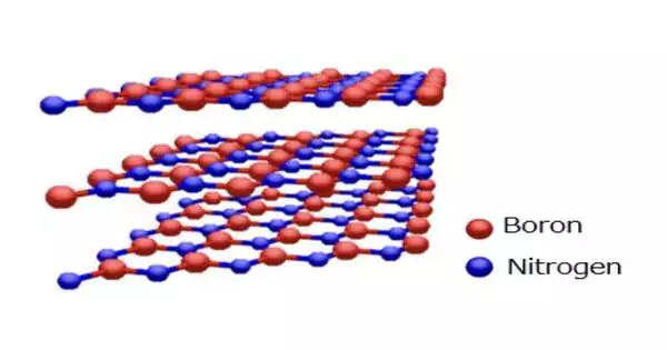
Scientists at Kyushu College, the Public Foundation of Cutting Edge Modern Science and Innovation (AIST), and Osaka College in Japan have as of late presented another system for blending multi-facet hexagonal boron nitride (hBN), a material that could be utilized to coordinate different 2D materials in electronic gadgets while saving their novel properties. Their proposed approach, framed in a paper distributed by Nature Gadgets, could work with the creation of new, profoundly performing graphene-based gadgets.
“The molecularly level 2D cover material hBN is a vital material for the mix of 2D materials into electronic gadgets,” Hiroki Back, one of the scientists who did the review, told Tech Xplore. “For instance, the most elevated transporter versatility in monolayer graphene is accomplished just when it is sandwiched by multi-facet hBN. Superconductivity seen in bent bilayer graphene likewise needs multi-facet hBN to detach from climate.”
Notwithstanding its incentive for creating graphene-based gadgets, hBN can likewise be utilized to coordinate transition metal dichalcogenides (TMDs) in gadgets, achieving solid photoluminescence and high transporter portability. It can likewise be important for leading examinations that zero in on moiré physical science.
In spite of its numerous potential purposes, up to this point the union of great HBN has ended up being testing, especially when contrasted with the blend of other 2D materials. The hBN created utilizing existing strategies is, by and large, excessively slim or not homogenous.
“Albeit promising outcomes have been accomplished utilizing compound fume affidavit (CVD), it is simply restricted to monolayer hBN, yet monolayer hBN isn’t adequately thick to screen out the natural impacts,” Back said. “Hence, controlling the thickness of hBN is as yet a test because of the intricate connections between the B and N species and the reactant substrate.”
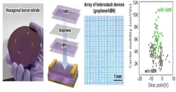
The vital goal of the new concentrate by Back and his partners was to recognize a system for creating hBN with a uniform thickness at various scales that addressed the issues of various gadgets. The group likewise wished to empower the fruitful mix of the blended hBN with graphene, achieving solid and profoundly performing gadgets at a wafer-scale.
The system they contrived depends on CVD, a compound cycle usually used to develop hBN and other 2D materials. While this cycle was applied in past works, it didn’t necessarily bring about homogenous and high-quality hBN.
“The cycle includes uncovering a metal substrate (polycrystalline Fe-Ni foil for our situation) to a gas containing the antecedents of the hBN (B and N), which go through compound responses at high temperatures to make layers of hBN on the outer layer of the Fe-Ni.” “By tuning the overall measure of Fe and Ni, a uniform isolation of hBN can be obtained.” Notwithstanding the CVD development, movement from the metal impetus is likewise vital, on the grounds that it firmly impacts the actual properties.”
To move the hBN they had developed onto graphene, Back and his partners utilized a material exchange method known as electrochemical delamination, utilizing H2 bubbles shaped at the connection point of the Fe-Ni and the hBN layers. While this cycle is known to be cleaner and more effective than other material exchange techniques, they tracked down that the connection point between the hBN and graphene layer was not as perfect as they would have liked and would hence not produce uniform graphene gadgets at a wafer scale.
“To resolve this issue, we efficiently concentrated on the impacts of different cleaning and treatment processes on the moved hBN and on the ensuing graphene,” Back said. “We found that successive toughening in a H2 climate at high temperatures guarantees somewhat clean connection points between the hBN and the graphene.”
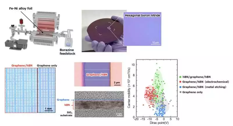
Utilizing their proposed hBN blend and move approach, the analysts had the option to create profoundly performing gadgets where graphene was typified by hBN. These gadgets were found to beat different gadgets in which graphene was put directly on a SiO2 layer.
“This exhibition improvement, which has recently been noticed for gadgets painstakingly designed in explicit, perfect, and homogeneous areas, was seen here interestingly for gadgets created at wafer-scale utilizing systems viable with large-scale manufacturing methods,” Back said. “We showed the fruitful blend of great hBN overall scales utilizing somewhat cheap Fe-Ni thwarts and created versatile exchange processes that empowered the manufacture of graphene gadgets with further developed execution at wafer-scale.”
This new concentrate by Back and his partners shows the capability of CVD-developed 2D materials for the large-scale manufacturing of profoundly performing and uniform gadgets. Later on, the system they created could be utilized to dependably deliver uniform hBN for a huge scope and afterward coordinate it in various gadgets.
Back and his partners presently plan to work on their union and move processes further to work with their presentation in both exploration and industry settings. For example, the hBN created during their tests shows a homogeneous thickness going between 5 and 10 nm across a wafer, which may not meet the necessities of especially intricate and requesting electronic applications.
“The capacity to create thicker hBN movies would result in better seclusion of other 2D materials, yet it has been shown to be trying to build the thickness while keeping up with the consistency,” Back added. “We are now attempting to further develop our union strategies. Furthermore, our ongoing exchange process depends on utilizing a PMMA conciliatory layer, so we are as of now examining elective strategies that result in cleaner moved hBN and that are more managable to modern scale handling, permitting to build the handling throughput while keeping up with the gadget quality.”
More information: Satoru Fukamachi et al, Large-area synthesis and transfer of multilayer hexagonal boron nitride for enhanced graphene device arrays, Nature Electronics (2023). DOI: 10.1038/s41928-022-00911-x


