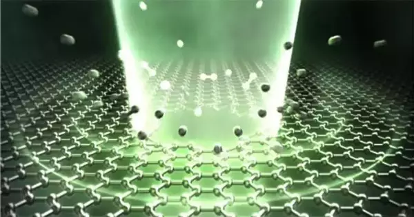
Graphene, which was discovered in 2004, has revolutionized numerous scientific fields. It has noteworthy properties like high electron portability, mechanical strength, and warm conductivity. Graphene-based transistors, transparent electrodes, and sensors were created as a result of extensive research into its potential as a next-generation semiconductor material.
However, effective processing methods that can structure graphene films at the micrometer and nanometer scales are essential for putting these devices to use. Nanolithography and focused ion beam techniques are typically used in the manufacturing of devices and micro- and nanoscale materials. However, laboratory researchers have faced difficulties with these for a long time because they require extensive equipment, lengthy manufacturing times, and complex operations.
A method that could micro/nanofabricate silicon nitride devices with thicknesses ranging from five to fifty nanometers was developed in January 2023 by researchers at Tohoku University. A femtosecond laser was used in the process, which produced extremely brief and rapid light pulses. It turned out to be able to process thin materials quickly and easily without using a vacuum.
“We deduced that the production of nanopores and defects could be controlled by utilizing a femtosecond laser irradiation after observing a tendency for the density of nanopores and defects to rise proportionally with the energy and number of laser shots.”
Yuuki Uesugi, assistant professor at Tohoku University’s Institute of Multidisciplinary Research for Advanced Materials.
The same group has now achieved multi-point hole drilling without causing damage to the graphene film by utilizing this strategy on an extremely thin atomic layer of graphene. On May 16, 2023, the details of their breakthrough were published in the journal Nano Letters.
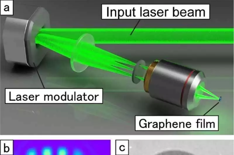
(a) The laser processing system’s schematic b) Development of 32 laser spots on the graphene film (c) Illustration of a multi-point hole-drilled graphene film Yuuki Uesugi et al.
“With legitimate control of the information energy and number of laser shots, we had the option to execute exact machining and make openings with distances across going from 70 nanometers (a lot more modest than the laser frequency of 520 nanometers) to north of one millimeter,” says Yuuki Uesugi, partner teacher at Tohoku College’s Establishment of Multidisciplinary Exploration for Cutting-edge Materials and co-creator of the paper.
Uesugi and his colleagues discovered that contaminants on the graphene had also been removed when they used a high-performance electron microscope to examine the areas that were irradiated with low-energy laser pulses that did not create holes. Further amplified perception uncovered nanopores under 10 nanometers in distance across and nuclear-level imperfections, where a few carbon molecules were absent in the precious stone designs of the graphene.
Depending on the application, graphene’s atomic defects can be advantageous or detrimental. Defects can improve or introduce new functionalities, as well as sometimes degrade particular properties.
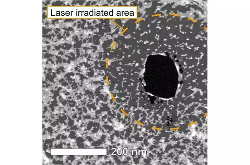
Scannable transmission Electron microscopy captured an image of a graphene film that had been processed with a laser. The dark regions demonstrate through-openings. The white items show surface foreign substances. credit: Yuuki Uesugi et al.
Uesugi adds, “We concluded the formation of nanopores and defects could be manipulated by using femtosecond laser irradiation.” “We observed a tendency for the density of nanopores and defects to increase proportionally with the energy and number of laser shots.”
“Graphene’s nanopores and atomic-level defects allow for the control of both quantum-level properties like spin and valley as well as electrical conductivity. In addition, this study’s contaminant removal by femtosecond laser irradiation may lead to the development of a novel, non-destructive, and clean method for washing high-purity graphene.”
In the future, the team intends to develop a laser-based cleaning method and conduct a comprehensive investigation into atomic defect formation. From the study of quantum materials to the development of biosensors, further breakthroughs will have a significant impact.
More information: Naohiro Kadoguchi et al, Nanoprocessing of Self-Suspended Monolayer Graphene and Defect Formation by Femtosecond-Laser Irradiation, Nano Letters (2023). DOI: 10.1021/acs.nanolett.3c00594


