The world’s first fully recyclable printed electronics were created by engineers at Duke University using water instead of chemicals during the fabrication process. The demonstration demonstrates a route that industry could take to lessen its impact on the environment and risks to human health by avoiding the need for dangerous chemicals.
It was published online on February 28 in the journal Nano Letters.
The ability to successfully secure multiple layers of components on top of each other, which is essential to creating complex devices, is one of the major challenges facing any electronics manufacturer. Particularly for printed electronics, getting these layers to adhere to one another can be challenging.
“Our thin-film transistors don’t match the best currently being manufactured, but they’re competitive enough to demonstrate to the research community that we should all be doing more work to make these processes more environmentally friendly,”
Aaron Franklin, the Addy Professor of Electrical and Computer Engineering at Duke,
The study’s principal investigator, Aaron Franklin, the Addy Professor of Electrical and Computer Engineering at Duke, said, “If you’re making a peanut butter and jelly sandwich, one layer on either slice of bread is easy.”. The jelly won’t stay put and will mix with the peanut butter if you spread the peanut butter on top of the jelly first, though. The process of building electronic devices with printing requires you to stack layers on top of one another, which is more difficult than just laying them down on their own.”.
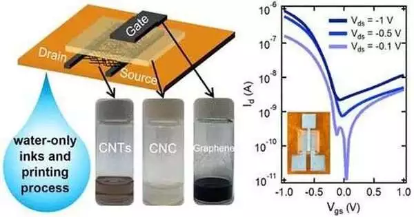
Franklin and his team have previously shown the first fully recyclable printed electronics. The devices made use of three carbon-based inks: insulating nanocellulose, semiconducting carbon nanotubes, and conductive graphene. The biggest obstacle to converting the original method to only use water was the carbon nanotubes.
A surfactant resembling detergent is added to create a water-based ink that allows the carbon nanotubes to spread evenly on a surface without clumping. However, the resulting ink fails to produce a layer of carbon nanotubes that is sufficiently dense for a strong current of electrons to pass through.
Franklin explained that the carbon nanotubes should resemble a bed of al dente spaghetti on a flat surface. “However, with a water-based ink, they appear to have been taken one by one and thrown against a wall to see if they were finished. If we were using chemicals, we could simply print multiple passes to generate enough nanotubes.Water, however, doesn’t function that way. The density would remain the same after 100 repetitions.”.
To create transistors that can be fully recycled using only water as opposed to harsh, toxic chemicals, an inkjet printer lays down layers of electronic ink based on carbon. Credit: Jason Arthurs Photography.
This is due to the surfactant that prevents the carbon nanotubes from clumping and also prevents subsequent layers from attaching to the first. The removal of these surfactants in a conventional manufacturing process would involve either extremely high temperatures, which consume a lot of energy, or harsh chemicals, which can be hazardous to both human and environmental health. Both were things Franklin and his crew wished to avoid.
In the paper, Franklin and his team describe a cyclical process in which the device is washed with water, dried at a low temperature, and then printed on once more. The researchers demonstrate that their inks and processes can produce fully functional, fully recyclable, fully water-based transistors by reducing the amount of surfactant used in the ink.
A transistor is a relatively complicated computer component that is used in devices like power control or logic circuits and sensors, in contrast to a resistor or capacitor. According to Franklin, by showcasing a transistor first, he hopes to show the rest of the field that there is a feasible way to make some electronics manufacturing processes significantly more environmentally friendly.
Franklin has already shown that nearly all of the carbon nanotubes and graphene used in printing can be recovered and used again in the same process with little loss of the materials or their performance viability. Nanocellulose can be easily recycled or degraded like paper because it is made of wood. However, compared to what is needed to deal with the toxic chemicals used in conventional fabrication methods, the process doesn’t use nearly as much water, despite the fact that it does use a lot of water.
Fewer than a quarter of the millions of pounds of electronics that are thrown away each year are recycled, according to a United Nations estimate. And as the world eventually switches to 6G devices, the issue will only worsen. Additionally, the Internet of Things (IoT) will keep growing. Therefore, it is crucial to make progress on any indentations that could be made in this mountainous pile of electronic waste.
Franklin claims that the method could be used in the production of other electronic components, such as the screens and displays that are now commonplace in society, although more research is necessary. A thin-film transistor backplane like the one shown in the paper is present in every electronic display. High-energy, toxic gases and risky chemicals are used in current fabrication technology. The US Environmental Protection Agency has declared the entire sector in need of immediate attention.
Though our thin-film transistors’ performance falls short of the best currently being produced, Franklin said they are still competitive enough to demonstrate to the research community that more needs to be done to make these manufacturing processes more environmentally friendly.
More information: Shiheng Lu et al, All-Carbon Thin-Film Transistors Using Water-Only Printing, Nano Letters (2023). DOI: 10.1021/acs.nanolett.2c04196


