Two-dimensional (2D) boron monosulfide (BS) nanosheets were created and characterized by researchers. A single BS nanosheet had higher band-gap energy than the bulk material from which it was formed. The band-gap energy eventually decreased to that of the bulk material as more 2D layers were stacked. The tunable electronic properties of BS nanosheets, which are suitable for electronic devices and photocatalytic applications, were reflected in this result.
Boron is a versatile nonmetal element, but scientists have only theorized about the useful properties and applications of two-dimensional (2D) boron-containing materials for the past five years. In a study published this month in the Journal of Materials Chemistry A, a team led by researchers from the University of Tsukuba put theory into practice by creating the first 2D boron mono sulfide (BS) nano sheets that can be handled layer by layer to control their electronic properties.
Our analysis confirmed what our own calculations had predicted. That is, BS nano sheets had different band-gap energy than the bulk material, and the bandgap could be tuned based on the number of stacked 2D BS sheets.
Professor Takahiro Kondo
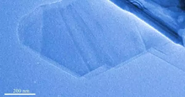
2D materials are good candidates for applications in batteries and other devices due to their large surface areas and diverse electronic states. Furthermore, combining 2D building blocks into novel materials can give you more control over their functionality. Previous computational studies indicated that BS, in particular, could adopt a number of stable 2D structures with distinct properties. As a result, the researchers created a 1:1 boron:sulfide bulk material with a rhombohedral (three-dimensional rhombus) crystal structure (r-BS), then removed individual nanolayers (2D BS), which preserved the original material’s crystalline arrangement.
“Our analysis confirmed what our own calculations had predicted,” says Professor Takahiro Kondo, leader of the research group. “That is, BS nanosheets had a different band-gap energy than the bulk material, and the band gap could be tuned based on the number of stacked 2D BS sheets.”
A material’s band-gap energy is related to its ability to conduct an electrical current, and it is thus a key property associated with potential electronic device applications. The band-gap energy of a single BS nanosheet was found to be relatively large, but it decreased as one or two additional nanosheet layers were added. After about five sheets were assembled, the stack’s band-gap energy eventually reached the level of the bulk r-BS.
“This feature, as well as the BS nano sheets’ low effective electron mass, indicated that they could potentially serve as n-type semiconductor materials with high conductivity,” Prof. Kondo explains, “which distinguishes them from other known 2D boron-containing materials that do not have band gaps.”
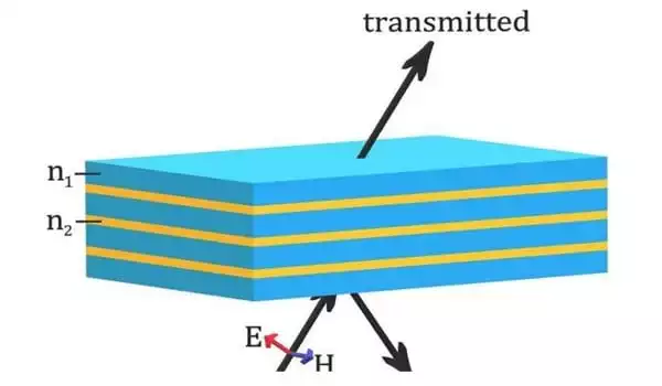
Electrodes made of r-BS or 2D BS responded to different wavelengths of light due to their distinct band-gap structures. To conduct a current and exhibit photocatalytic behavior, the r-BS required lower-energy irradiation (i.e., visible light), whereas the larger band gap of the 2D BS was only active under higher-energy ultraviolet light.
Boron is anything but dull! These light-induced phenomena demonstrated that 2D boron mono sulfide materials can be used in photocatalytic or electronic devices, and that their properties can be tuned as needed by varying the number of nano sheets.
Intercalation and pillaring reactions produce materials with useful properties for catalysis, electrodes for Li batteries, and adsorbents from layering materials with intra-crystalline reactivity. The layered structures capable of delamination revealed new applications for layered inorganic solids. Exfoliated particles are thought to be a new type of nanomaterial based on single crystal nano sheets. These nano sheets can be used as building blocks for nanomaterials with novel properties due to their distinct morphological features and properties.


