Optoelectronics identify or produce light and are utilized in various gadgets in a wide range of businesses. These gadgets have generally depended on meager semiconductors, which are little semiconductors that control the development of electrons and photons made from graphene and other two-layered materials. In any case, graphene and these different materials frequently dislike band hole opening and have different weaknesses that have scientists looking for another option.
When treated with a strategy called the Lewis corrosive treatment, palladium diselenide is a potential answer for fulfilling the necessities of optoelectronic gadgets.
Research dissecting this technique was distributed in a paper in Nano Exploration.
Prof. Dr. Mark H. Rümmeli, Time Seats teacher at the Specialized College of Ostrava (VSB-TUO), said, “Palladium diselenide shows exceptional actual properties, including a tunable band hole and noteworthy gadget execution. Remarkably, it exhibits long-haul dependability in surrounding air without the requirement for extra bundling.”
“Palladium diselenide has unique physical properties, such as a tunable band gap and outstanding device performance. Notably, it exhibits long-term stability in ambient air without further packaging.”
Prof. Dr. Mark H. Rümmeli, ERA Chairs professor at the Technical University of Ostrava (VSB-TUO).
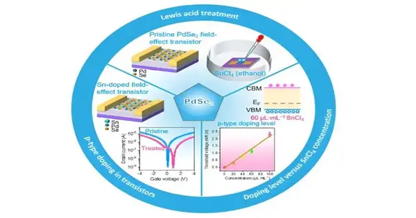
Enlivened by semiconductor material science, the scientists thought about how doping could modify palladium diselenide to work on its presentation. Doping is the deliberate acquaintance of debasements with a material, bringing about three sorts of materials: flawless, p-type doped, and n-type doped. Whenever a p-type doped material and a n-type doped material touch, they make a p-n intersection. This intersection is fundamental for optoelectronic gadgets since it is where light-to-electron and electron-to-light change happens.
To make p-type doped and n-type doped palladium diselenide in a controlled design, specialists utilized the Lewis corrosive treatment. “The controlled degree of doping can make palladium diselenide have an alternate energy bandgap, which enhances a toolbox or library of materials for the choice and plan of the p-n intersection,” said Dr. Hong Liu, a teacher at the State Key Research facility of Precious Stone Materials at Shandong College in Jinan, China.
“The Lewis corrosive treatment can present the replacement of the palladium iotas (by tin from tin chloride, one kind of Lewis corrosive) in the palladium diselenide. We found an information-fitting condition between the doping level and the convergence of Lewis corrosive, which might rouse individuals to control more p-type doped two-layered materials.”
To test this strategy, specialists arranged a perfect film of palladium diselenide. The film was then changed using the Lewis corrosive treatment. After the underlying Lewis corrosive treatment, the cross-section construction of the palladium diselenide film was unaltered, yet the arising pinnacles of tin, palladium, and selenium were affirmed utilizing imaging.
These pinnacles demonstrated that tin could be utilized as a p-type dopant. An extra trial of various convergences of tin chloride showed how the limit voltage of the palladium diselenide could be controlled based on the grouping of the tin chloride. These rules can be applied for future doping of palladium diselenide utilizing Lewis acids. It could likewise give an outline of how to do comparable testing on other semiconductor materials.
Looking forward, analysts will arrange for how to scale the handling of these two-layered materials. “We will show the thrilling utilization of p-type doped palladium diselenide in a few electronic parts, for example, field-impact semiconductors, photodetectors, and light producers. We intend to attempt to streamline the semiconductor doping strategy, which can be promptly taken on by modern guidelines and could be utilized in the semiconductor business for large-scale manufacturing sooner rather than later.”
“Our definitive objective is to apply this strategy in wearable and adaptable gadgets by coordinating the palladium diselenide-based semiconductors and photodetectors with polymer-based strain sensors in adaptable substrates, which bring about a savvy biomedical framework for human medical care checking applications,” said Dr. Jinbo Ache, a teacher of science and materials science at the College of Jinan in Jinan, China.
More information: Jiali Yang et al. Modulating p-type doping of the two-dimensional material palladium diselenide, Nano Research (2023). DOI: 10.1007/s12274-023-6196-7


