Electronic gadgets are evolving. Foldable phones, rollable electronic watches with wraparound displays, and extensible displays with wider screens have all made their way into our lives. Is it possible to have a display that folds up like paper and fits in our pockets?
The pieces of such deformable devices must also be flexible. However, the underlying technology for an interface material that joins different sections is still unknown. A POSTECH research team has created a malleable conductive layer that links flexible electrical components in response to this.
Stretchy conductors have become an important building block for connecting the working circuits of a variety of stretchable electronics. Stretchy heaters, stretchable energy conversion and storage devices, stretchable transistors, sensors, and artificial skin are among the several stretchable electronic devices that have been developed as a result of the success of stretchable conductors.
We anticipate this research to be a prime example of a bold investment in basic research leading to commercialization.
Professor Unyong Jeong
A research team led by Professor Unyong Jeong and Ph.D. candidates Hyejin Hwang and Minsik Kong of Department of Materials Science and Engineering in collaboration with Professor Ho-Jin Song of Department of Electrical Engineering and Professor Soojin Park of Department of Chemistry at POSTECH have together developed a stretchable anisotropic conductive film (S-ACF) that can connect other electrodes physically and electrically regardless of the rigidity, flexibility or elasticity of the circuit line. This study’s findings were published in Science Advances, a prestigious international magazine.
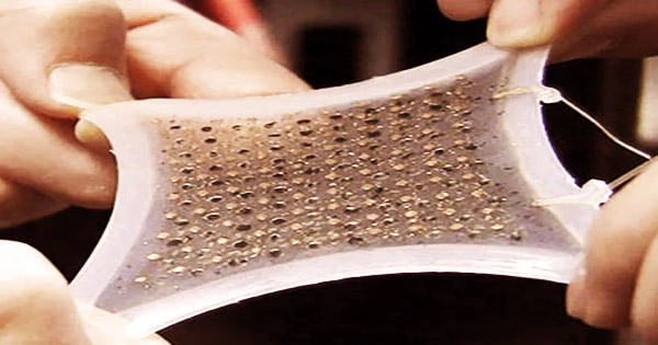
A deformable circuit board is required for stretchy devices such as stretchable screens, electronic skin, and implantable devices. Many materials and components, including as wirings, displays, and sensors, as well as rechargeable energy supply devices such as batteries, are required for circuit boards that may be shaped into various forms.
Soldering, wire bonding, an anisotropic conductive film, and flip-chip bonding have all been used to link high-resolution circuits so far, but there is still the problem of retaining the physical and electrical characteristics of the circuits when their form is changed.
The researchers achieved this by placing metal particles at regular intervals in SEBS-g-MA, an extensible block copolymer that maintains high interfacial adhesion while providing stable electrical connections even when its form is modified by chemical bonding with the substrates. Due to the promise of wearable electronic systems, the continuing development of stretchy electronics has led to the new functionality of transparency, and the fabrication of transparent stretchable electronic devices has received a lot of interest.
Maleic anhydride, which is contained in SEBS-g-MA, allows for chemical interaction between substrates, resulting in robust adhesion even at low temperatures. When the S-ACF was put at the contact interface between the two substrates with mild temperature (80°C) treatment for around 10 minutes, the researchers verified that the electrical and physical connection was effectively created.
Furthermore, S-ACF may be selectively engineered to arrange particles in the desired section, increasing the polymer contact surface in areas that do not require electrical connection to boost bonding strength and saving money by lowering the use of metal particles. This film adds stretchability to traditional anisotropic conductive films and allows for high-resolution circuit connections (50m), low-temperature manufacturing, and production scalability.
“This film enables connecting devices with more complex structures in the future,” explained Professor Unyong Jung who led the study. He added, “I hope that it will serve as a launchpad for integrating and manufacturing stretchable devices which have been independently studied into one substrate and integrated system.”
Wouldn’t it be conceivable to link stretchy high-resolution circuits with a little piece of tape if S-ACFs were to be made as tapes in the future?
From 2014 through 2018, the Samsung Future Technology Development Project provided long-term assistance for foundational research on the arrangement of conductive microparticles, enabling the start-debut up’s and eventual technology transfer. The project has been selected as a Materials & Components Technology Development Program by the Korea Evaluation Institute of Industrial Technology (KEIT) and is awaiting domestic production of high-precision anisotropic conductive films as a result of additional research and development for commercialization.
Professor Jeong commented, “We anticipate this research to be a prime example of a bold investment in basic research leading to commercialization.”
The National Research Foundation of Korea supported this study with funding from the Nano and Material Technology Development Program.

