The new findings used a cleaner technique to manipulate the flow of electricity, giving graphene greater conductivity than metals like copper and gold and increasing its potential for use in telecommunications systems and quantum computers.
The silicon revolution gave birth to the device on which you are currently reading this article. Researchers control silicon’s current-conducting capabilities via doping, which is a process that introduces either negatively charged electrons or positively charged “holes” where electrons used to be. This allows for the control of the flow of electricity, and for silicon, this entails injecting other atomic elements that can adjust electrons, known as dopants, into its three-dimensional (3D) atomic lattice.
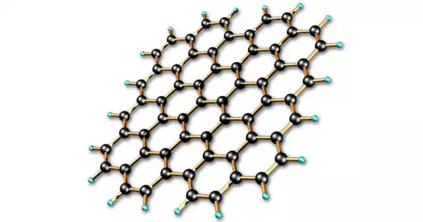
However, the 3D lattice of silicon is too large for next-generation electronics such as ultra-thin transistors, new optical communication devices, and flexible bio-sensors that can be worn or implanted in the human body. Researchers are experimenting with materials no thicker than a single sheet of atoms, such as graphene, to thin things out. However, the tried-and-true method for doping 3D silicon does not work with 2D graphene, which is made up of a single layer of carbon atoms and does not normally conduct current.
It is a clean method for doping graphene using a charge-transfer layer made of low-impurity tungsten oxyselenide. This is a novel method for tailoring the properties of graphene on demand. We’ve only just begun to investigate the possibilities of this new technique.
James Hone
Rather than injecting dopants, researchers attempted to layer on a “charge-transfer layer” designed to add or remove electrons from graphene. Previous methods, on the other hand, used “dirty” materials in their charge-transfer layers, which left the graphene unevenly doped and hampered its ability to conduct electricity.
A new study published in Nature Electronics proposes a better way. An interdisciplinary team of researchers led by James Hone and James Teherani of Columbia University and Won Jong Yoo of Sungkyunkwan University in Korea describe a clean method for doping graphene using a charge-transfer layer made of low-impurity tungsten oxyselenide (TOS).
The new “clean” layer was created by oxidizing a single atomic layer of tungsten selenide, another 2D material. They discovered that when TOS was layered on top of graphene, it left the graphene riddled with electricity-conducting holes. By sandwiching a few atomic layers of tungsten selenide between the TOS and the graphene, those holes could be fine-tuned to better control the materials’ electricity-conducting properties.
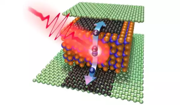
The researchers discovered that their new doping method increased graphene’s electrical mobility, or how easily charges move through it, compared to previous attempts. Adding tungsten selenide spacers increased mobility to the point where the effect of the TOS is negligible, leaving mobility to be determined by graphene’s intrinsic properties. Graphene’s electrical conductivity is higher than that of highly conductive metals such as copper and gold due to the combination of high doping and high mobility.
According to the researchers, as the doped graphene improved in its ability to conduct electricity, it also became more transparent. This is due to Pauli blocking, a phenomenon in which doped charges prevent the material from absorbing light. Graphene became more than 99 percent transparent at infrared wavelengths used in telecommunications. It is critical to achieve a high rate of transparency and conductivity when moving information through light-based photonic devices. Information is lost when too much light is absorbed.
The researchers discovered that TOS-doped graphene has a much lower loss than other conductors, implying that this method has the potential to be used in next-generation ultra-efficient photonic devices. “This is a novel method for tailoring the properties of graphene on demand,” Hone explained. “We’ve only just begun to investigate the possibilities of this new technique.”
One promising direction is to change the pattern of the TOS to alter graphene’s electronic and optical properties, as well as to imprint electrical circuits directly on the graphene itself. The team is also working on incorporating the doped material into novel photonic devices, which could be used in transparent electronics, telecommunications systems, and quantum computers.
