Material flakes in two dimensions, or 2Ds, have extraordinary quantum properties that are not found in everyday materials because they are composed of just one or a few atomic layers. Consequently, these materials have enormous potential for advanced research and industrial applications.
In the past, ellipsometry has been a popular optical method for measuring thin-film thicknesses without using any tools. However, 2D flakes frequently have lateral dimensions of only a few microns, and commercial ellipsometers are limited in their ability to measure areas smaller than 50–60 microns.
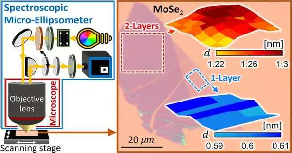
A system and method for a microscope-integrated ellipsometer, known as the Spectroscopic Micro-Ellipsometer (SME), have been developed and patented by Prof. Ronen Rapaport and Ralfy Kenaz of Hebrew University to address this significant obstacle.
In just a few seconds, this cutting-edge instrument can measure thin-film thicknesses in extremely small areas down to just 2 microns wide with atomic-level precision. A separate publication has already confirmed the instrument’s exceptional performance, establishing its credibility and dependability.
Hebrew University researchers used this cutting-edge micro-ellipsometer to solve the current scientific problem of measuring and mapping the thicknesses of atomically thin 2D material flakes in a recent publication in the journal ACS Nano. The micro-ellipsometer’s ability to successfully measure and map the thicknesses of various 2D material flakes, allowing for the determination of their number of atomic layers, is unequivocally demonstrated by the findings.
This research has repercussions for a wide range of microstructure-related businesses and research areas. It also paves the way for highly precise optical investigations of microstructures, paving the way for technological and scientific advancements. This study presents a novel and valuable system for researchers and businesses alike by introducing the application of the well-established and highly sensitive ellipsometry method to microstructures.
The Spectroscopic Micro-Ellipsometer can be used in the thin film industry to control wafer quality, study the crystal structure of nanoparticles, characterize nanoscale metamaterials and 2D devices, and more.
More information: Ralfy Kenaz et al, Thickness Mapping and Layer Number Identification of Exfoliated van der Waals Materials by Fourier Imaging Micro-Ellipsometry, ACS Nano (2023). DOI: 10.1021/acsnano.2c12773
