The industrial supply of molybdenum disulfide (MoS2), a next-generation two-dimensional (2D) semiconductor, is likely to be built on a large-scale (4-inch) plasma etching technology that has been developed.
“large-scale (4-inch) atomic layer etching technology for MoS2, a next-generation semiconductor, using plasma-based reactive ion etcher (RIE) equipment,” according to the joint research team led by Professor Taesung Kim of Sungkyunkwan University and led by Senior Researcher Hyeong-U Kim of the Department of Plasma Engineering at the Korea Institute of Machinery and Materials (KIMM).
As co-first authors, senior researcher Muyoung Kim and postdoctoral researcher Changmin Kim of KIMM contributed to this study, which will appear in the February 2023 issue of Chemistry of Materials as the cover article.
It is necessary to control the manufacturing process on an atomic level as the line width of conventional silicon-based semiconductors gradually decreases.
“AI, GPT, IoT, self-driving, cloud, and other future industries fall into the category of non-memory sectors. As a result, even Samsung Electronics, the market leader in memory, has been focusing its investments on the foundry sector.”
Senior Researcher Hyeong-U Kim of KIMM who led the research
However, the tunneling effect caused by the accumulation of atomic layers makes it difficult to precisely process the single atomic layer of silicon-based semiconductors. As a result, developing new materials for the semiconductors of the future has become a necessity.
In contrast, even in a structure with a thickness of one nanometer (nm), MoS2 allows for stable control of electron movement without tunneling. As a result, MoS2 has been drawing attention as a promising new material that has the potential to overcome the limitations of semiconductors based on silicon.
However, the development of MoS2-based semiconductors has remained at the basic research stage in laboratories due to the difficulty of uniformly forming MoS2 at large scales for mass manufacturing, despite the fact that MoS2 has superior electric and physical properties to silicon, even in terms of atomic layer thickness.
In particular, despite the fact that semiconductor precision necessitates the formation of a layer the thickness of a single atom, the lack of technology for precisely etching MoS2 into atomic layers prevented the commercialization of MoS2.
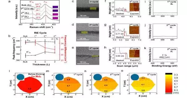
Using the two plasma processes of plasma-enhanced chemical vapor deposition (PECVD) and RIE, a method that allows the etching of large-scale (4-inch) MoS2 to the desired atomic layer thickness has been developed for the first time in this study. Consequently, the research has opened up new possibilities for the industrial application of semiconductors based on MoS2.
The plasma etching process has received a lot of attention because it is the most likely technology that could surpass conventional etching processes. However, one of the main drawbacks of plasma etching is that after the process, impurities (fluorine, F) remain on the semiconductor’s surface; consequently, additional steps are required to remove these residues. As a result, it has long been a goal to achieve both atomic-level precision and ultrahigh purity in MoS2 layers through highly complex plasma process design.
Using a density functional theory (DFT)-based computational screening system, the team at the most recent study was able to address these issues. The cutting-edge computational screening system that simulated the surface reaction of candidate gases and combined the best gas mixture for ultrafine process quality was proposed by Muyoung Kim, Ph.D., one of the co-first authors. When compared to conventional experiment-based manufacturing, this strategy’s screening system significantly reduces plasma process development time and costs. He focused specifically on the atomistic mechanism of the surface reaction and discovered the function of the process gas on the MoS2 substrate, thereby justifying the mixed-gas recipe (Ar + O2 + CF4).
“future industries such as AI, GPT, IoT, self-driving, cloud, etc.,” stated Senior Researcher Hyeong-U Kim of KIMM, who led the research. All of them are classified as non-memory sectors. As a result, even Samsung Electronics, the market leader in memory, has been concentrating its investments on the foundry industry. The foundry process seeks limited production of diverse items, whereas the semiconductor memory manufacturing process has focused on mass production of limited items. As a result, processes that can control fine line widths have become more and more important, particularly in the foundry process.”
Kim continued, “It is necessary to develop processes where even single-atomic layers are controllable, as demonstrated in our latest research, to overcome the limitations of integration.” As a result, numerous studies have been carried out since roughly a decade ago. However, prior to our most recent research, no one had been able to show that it was possible to uniformly and consistently etch atomic layers on a large scale. The outcome of our research is expected to assist the non-memory 2D semiconductor industry in the future in making a new breakthrough.”
More information: Changmin Kim et al, First-Principles Calculation Guided High-Purity Layer Control of 4 in. MoS2 by Plasma RIE, Chemistry of Materials (2023). DOI: 10.1021/acs.chemmater.2c02914


