It is anticipated that two-dimensional materials will revolutionize the semiconductor industry. However, despite the fact that a number of studies have reported prototype devices with promising properties for sensing and driving electrical current, their technology readiness level is still very low due to the fact that most of them use synthesis and processing techniques that are incompatible with industry, produce large devices on substrates that are not functional, and present poor yield and variability.
Dr. Mario Lanza, associate professor of materials science and engineering at King Abdullah University of Science and Technology (KAUST), leads a group of researchers who have successfully integrated two-dimensional materials onto silicon microchips with excellent integration density, electronic performance, and yield. The review has been distributed in Nature.
According to Lanza, “the majority of microchips in the future will exploit some of the many outstanding electronic and thermal properties of these materials.”
“In the future, most microchips will take advantage of some of these materials’ many remarkable electrical and thermal capabilities.”
Dr. Mario Lanza, associate professor of materials science and engineering,
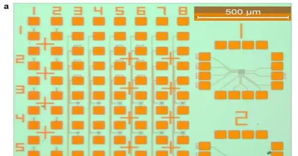
Multilayer hexagonal boron nitride, a two-dimensional insulating material about 6 nanometers thick, was used by Lanza’s team to use silicon transistors from complementary metal-oxide-semiconductor (CMOS) technology, which is used in every electronic device we use, including phones, computers, automobiles, medical devices, and household appliances.
The hybrid 2D/CMOS microchips that result have special electronic properties and a high degree of durability, making it possible to create artificial neural networks with very little power consumption. They are able to successfully compute spiking neural networks, which are essential parts of current artificial intelligence systems that are becoming increasingly in demand. Spiking neural networks are made up of electrical stresses applied over very short periods of time. The latest gadgets are not reasonable for carrying out this sort of brain organization, and there is a market need to track down new methodologies.
Numerous semiconductor companies have expressed an interest in the research, which has the potential to assist other businesses in lowering energy and processing costs. The majority of businesses in artificial intelligence and microchip manufacturing want to develop new hardware that can speed up data processing and save energy, but they haven’t yet found a device that works well.
For radio-frequency applications, IBM attempted to incorporate graphene into transistors, but the devices were unable to store or process information. Interestingly, the gadgets made by Teacher Lanza’s group measure just 260 nanometers and could be made a lot more modest effectively in the event that further developed computer chips were accessible.
This work is energizing for the field of nanoelectronics and semiconductors on account of the elite exhibition of the gadgets and circuits delivered and the potential for sweeping industry applications.
More information: Kaichen Zhu et al, Hybrid 2D/CMOS microchips for memristive applications, Nature (2023). DOI: 10.1038/s41586-023-05973-1


